Hi DadoThe second one, same input voltage.
dado
you have got great results with hudge dc offset

anyway I like more the first sch but I am more impressed of the second
Hi Dado
you have got great results with hudge dc offset
anyway I like more the first sch but I am more impressed of the second
Yes I know about the offset. I think it was a problem with LTspice models for BC transistors. Here is a simulation with Cordell's models and the offset is a way down. Nice think about this lineamp is that is non inverting.
Damir
Attachments
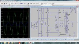
... Nice think about this lineamp is that is non inverting. Damir
I read that the engineers like to invert the signal
but indeed it is very good lineamp.
what do you think about RIAA section instead of R1C2?
will it have sufficient gain and minimal noise?
 asc file would be very helpful
Last edited:
I read that the engineers like to invert the signal
but indeed it is very good lineamp.
what do you think about RIAA section instead of R1C2?
will it have sufficient gain and minimal noise?
I don't think this amp could be used as RIAA amp, but I have to think about it a bit more.
The ratio R1/R9 together with CM's ratio define the gain, as this is a current conveyor.
Damir
The gain resistor could be replaced with an RIAA stage, but without offset control you would not get much gain.
However you could easily use this circuit as an active crossover, with the gain resistor split into multiple crossover networks going to different buffers. I think this would be superior to a voltage-drive active crossover, not that I really know anything about active crossovers.
However you could easily use this circuit as an active crossover, with the gain resistor split into multiple crossover networks going to different buffers. I think this would be superior to a voltage-drive active crossover, not that I really know anything about active crossovers.
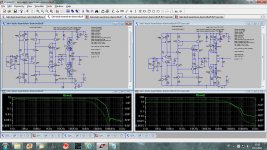
To convert conveyor output current to voltage it uses a resistor and that voltage should be buffered against output load. First output buffer I used was JLH buffer with floating cascode. As the cascode transistor it uses JFET and power voltage is limited by used JFETs.
Here I used BJT as floating cascode and this allows higher power voltage to be used and as a consequence higher output voltage with very similar distortion figures.
There are comparison between JFET cascoded buffer with gain of 7 and BJT cascoded buffer, with gain of 9 and the power voltage of +-40 V instead of +-30 V. Input was 1 ppV.
dado
Attachments
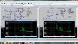
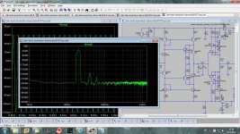
This line amp could be called "wire with gain" as it has so low distortion(simulated).
Below are FFTs at the output voltages used mostly at listening.
dado

This line amp could be called "wire with gain" as it has so low distortion(simulated).
Below are FFTs at the output voltages used mostly at listening.
dado
respect,
did you build it already?
respect,
did you build it already?
No, not yet.
practical implementation
My Lineamp is ready to be build and tried in my system.
I made three different schematic, but I will try one of them. All three simulate very similar but I will make this one to see how it sounds.
Here is PCB layout I am going to make. Any suggestion for improvement is appreciated.
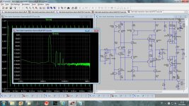
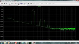
Distortion(simulated) is very low and here is FFT for 20kHz and at 3.2 v p2p.
dado
My Lineamp is ready to be build and tried in my system.
I made three different schematic, but I will try one of them. All three simulate very similar but I will make this one to see how it sounds.
Here is PCB layout I am going to make. Any suggestion for improvement is appreciated.
Distortion(simulated) is very low and here is FFT for 20kHz and at 3.2 v p2p.
dado
Attachments
![GainWire-2SA-2SC-JFET.LAY].jpg](/community/data/attachments/298/298167-cfe62dce3675b20a8d39811f2f6c4185.jpg)
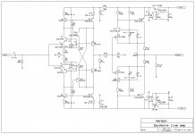
Here are two more schematics, one for low voltage and very similar distortion pattern. Very important thing(in my opinion) is uniform distortion throughout whole bandwidth. With my first version, I hope I can drive 300 ohm headphones with easy(even with 30 ohm it is quite good with some more distortion).
dado
dado
Attachments
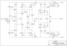
Why are you using the A970/C2240? These will in all likelihood mess up those low THD figures. Use the OnSemi BC327/337 (if not, the BC5xx). I've proven these transistors to have good low-Vce behavior. Q1/2/5/7/9/10 (first schematic) all need to be low-quasisat types.
Because I have those transistors at home, latter I could order the types you suggested.
Could you suggest from were to order.
I am curious whay you do not like A970/C2240, I have good experiance with them??
dado
It's not that I don't like them, they just are not right for the application. High-voltage transistors typically do bad at low-Vce. Thus it is a good idea to always avoid high-voltage BJTs in current mirrors. The BC327/337 have low internal resistance and great Vcesat behavior (the OnSemi ones did, but not NXP IIRC, haven't tested Fairchild but I would think they are okay). Thus they are pretty much perfect for a current mirror. The SMD dual versions would be perfect. Furthermore I have measured a number of BC series transistors and they are mostly matched within 300uV IIRC (this was for BC560C). A smaller test with the BC3x7 suggested they are no different.
The A970/C2240 have relatively good Vcesat behavior, but I would rather use them where they work best, in input stages.
The A970/C2240 have relatively good Vcesat behavior, but I would rather use them where they work best, in input stages.
Last edited:
It is supposed to improve PSRR. Edmund uses a similar technique in his Super TIS. It conserves the rail-modulated currents through the 150k resistors, and combines them so they cancel. I seem to recall that in the original configuration, asymmetric rail variations would cause higher PSRR than normal. Forcing the 150k resistor current to flow through both loops caused asymmetric PSRR to improve. But I also seem to recall there were some innocent gaffes made on that part of the circuit that got corrected later.
Probably. I don't have any models for those transistors, because I've tested the models and found they are not anything like the real devices. In simulation it is better to use an inferior part with an accurate model, than to use a superior part with an inferior model. Else you'll just mislead yourself and anyone who trusts your skill.
- Status
- This old topic is closed. If you want to reopen this topic, contact a moderator using the "Report Post" button.
- Home
- Source & Line
- Analog Line Level
- Current conveyor as a voltage amplifier