@dirk: nice job
L.
Gee thanks. Considering my lack of experience, that's a fine compliment.
")
If you can't get the parts, find a good IC.
For the record, I did a simple Google search for two complementary jfets, the J113 and the J175. I found both of them for sale under $0.50 each. You just have to buy a bunch of them and select them out. If you cannot invest $100 for this, then buy an IC. It will give you better performance.
Yeah, unfortunately you're right. An LME49710 + LME49600 will do this job just fine and take up less space, but it's just not fun or a challenge.
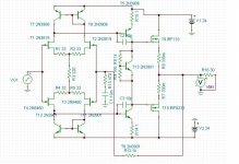
This is a recommended alternative to a complementary differential fet design. This design was used in several professional mixers as well as in three 30ips master analog recorders.
sorry about the bad copy, the original schematic goes back to about 1977.
I quite like this, but the FET output stage is a bit idiosyncratic for my liking. You could use a FET source follower with a BIP current source load for true class A output? No need to skimp on the supply current - this is DIY.
I juiced up the whole thing and distortion is now 0.0005% @ 20kHz into 30 ohms @ 1.1Vrms. DC offset on the output is -1mV.
I have since added Miller capacitors (@10pF each) to get rid of a 15dB spike @ 10MHz. Distortion is now 0.0006% under the above conditions. S/N is 120dB @ 10kHz.
Unfortunately, large heatsinks are required on the outputs.
Finally, something I understand.
Nice!
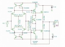
For the sake of circuitry discussions, this one from John Linsley Hood I found in my archive.
Patrick
OH! I'm going to try a variation on that! thanky thanky!
Would you elaborate ?Yes, these are the devices. Many manufacturers still make them. However, they have a LARGE Idss spread, so only dumb luck will match the P's to the N's, but that is not very important, within limits. Just good N to N, and P to P is the most critical.
It would seem to me N to P would be more important
than N to N and/or P to P ?
At least, if the two output devices are reasonably well-matched, and perhaps with some ballasting R in the sources, the quiescent bias can be not too unstable.
Not enough. Thermal dependence of current of 1'st stage (diff-pair + current source in the tail) is amplified by the 2'nd stage, and thermal dependence of it's current _added_ to it.
This is a recommended alternative to a complementary differential fet design. This design was used in several professional mixers as well as in three 30ips master analog recorders.
sorry about the bad copy, the original schematic goes back to about 1977.
I think I'd start with this one, with updated JFETs. The output stage can use a J202 (maybe with a 2n5461 as the p-ch compliment), perhaps with cascoded drains to increase the rail voltage capability, a la Burson HD/OPA-Earth.
The input stage can be bipolar (2sc1845, etc.) or cascoded 2sk170. Also worth looking at is the Toshiba 2sk241 small-signal depletion-mode MOSFET for the input stage - low Vdsmax makes a cascode mandatory.
Last edited:
John,
Would you care to comment on the topology in post#306 ?
Please ignore the devices. They are of course not up to date.
Some specific questions :
1. Is the current mirror of the first stage really necessary ?
Could we not just tape the drive voltage to the 2nd stage off the resistors (if necessary different values) ?
2. Cascode vs no cascode for 2nd stage ?
Are the cascode there for open loop frequency response reasons ?
Thanks,
Patrick
Last edited:

I wish you'd stop calling me Surely.
At wafer probe, the probe setup can be used to test adjacent die, and they can setup the inker to either mark the good pairs, or mark those which do not meet requirements. Subsequent auto pick and place can easily visually detect either lack of an ink dot, or a specific color.(although until Scott posted I had no idea what they really did, but knew that positional adjacency information was either lost or not taken into account).
After test, the wafer is first bonded to a sticky plastic film, the either scribed and broked like Scott mentions, or the wafer is sawcut between the die to the film as I've been involved with. The "expanded" I mentioned is a film which can be stretched, and a rounded probe under the die can push up so that the film releases the die to the vacuum pick.
My work back in the day was with mil spec hybrids, so laser scribing was a definite no-no...we had to pass PIND testing.What's funny is that back in 1974 they had a slice of a huge steel rod about 4" in diameter that they rolled over the wafer to break all the scribes.
jn
How can the die be attached to the collector/drain/source?
How many layers are in that connection?
A wafer backside is generally the collector for power zistors, and drain for power fets.
Small signal devices can be isolated from backside by a reverse biased pn junction, or even a grown isolation like silicon nitride.
My work with individual or dual transistors/fets had only the one layer of aluminum in a 2-d pattern.. MSI and LSI of course had multiple layers with crossovers. Copper traces weren't around in my day, we had to fight the raptors..
John
Dirk, maybe the peak goes away when you make an output inclusive compensation.
Yeah, about 13pF put across the feedback resistor brings the spike down to about 6dB (from 15 or so). Distortion is slightly worse though. Someone else needs to step up and start modeling. Too much yapping about dies and other things and not enough modeling!
- Home
- Source & Line
- Analog Line Level
- Discrete Opamp Open Design