Let me clarify things for you all: Over the decades, I have had a series of 'requirements' for making an audio gain stage, developed after years of making prototypes. This designs meets MY criteria, but then I designed the whole thing and put it into a power amplfier, 30 years ago. I guess I should mention that, but that is NOT why I said that it was 'rational'. I meant that this design example meets MY criteria, and does not fall down in some way. Now, if I am allowed, I will try to show where many other designs fall away from meeting the criteria that I find useful and important. Not ALL designs are failures in some way, but they have yet not been presented here to any degree, recently.
Thanks! Now I know to what you were referring.
I wish you'd stop calling me Surely.
No, I was speaking with poetic license (although until Scott posted I had no idea what they really did, but knew that positional adjacency information was either lost or not taken into account).
What's funny is that back in 1974 they had a slice of a huge steel rod about 4" in diameter that they rolled over the wafer to break all the scribes.
I bet this was the answer everybody was seeking for...
In addition to Ken's question, I am wondering whether the natural output impedance (without feedback) is low enough to be called a OP amp output stage. To me it appears more like both output MosFets would act like inverse controlled currents sources and consequently would deliver a high output impedance.
...on the other hand, there is no proof that only circuits with a natural low output impedance sound good.
Yes, that's how the output stage appears to operate to me as well. It seems the totem pole output is designed as a high impedance node, not the current-source loaded follower it might appear to be on first glance. This was the design aspect I was most hoping John might speak to. Lowering of the output impedance would (I presume) come via negative-feedback. If the output does in fact behave like a high impedance transconductance node, I wonder how it might perform using a simple I/V gain setting resistor connected to ground, without a negative feedback loop.
Last edited:
Please tell Wavebourn what you found, Ken! '-)
I am eager to know! Did he found that differential pair of MOSFETs loaded on many times different resistances does not exhibit 2'nd order distortions? Or did he found that as drawn that amp will be quite thermally stable?
")
By the way, I was thinking about thermal stability issue yesterday, and found some ideas.
What's funny is that back in 1974 they had a slice of a huge steel rod about 4" in diameter that they rolled over the wafer to break all the scribes.
I heard an anecdote in 1970'th that some Japanese company was buying lots of Soviet transistors that were not used in their production. It turned to be, they cleaned dies to make many transistors from one, and melted cases on scrap metal.
One more Soviet anecdote. When Shokin become Minister of Electronic Industry, visiting one plant he spotted a huge red banner above the entrance, "Praise Soviet Transistors, the Biggest Transistors in the World!" He whispered, "Remove that shame immediately!"
Please tell Wavebourn what you found, Ken! '-)
Huh?
What did I find?
I wonder how it might perform using a simple I/V gain setting resistor connected to ground, without a negative feedback loop.
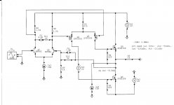
Speaking now of the Constellation-like simplified schematic from JC's post #168:
Too much gain for open loop, without a lot of local feedback/degeneration.
As an amp around which feedback will be applied:
The concerns about output impedance and stability are well-taken, but there are ~fixes.
For an example I threw down of BF862 input pair, ZVP3306 second stage pair, and ZVN3306 ouputs, 10mA in input tail, 10mA each in P channel, 220 ohm bias R across each output G-S. I see an open loop output impedance resistive to about 92kHz of 2.1k ohms. But one of the problems is that the lower output device must supply all of the input bias current of the upper device, so this intrinsically unbalances the P pair. Throw down a current sink from the output (or just a resistor to the negative rail), then the second stage can be balanced. It's also good to put some voltage drop in the one drain to equalize the drain voltages of the P devices.
Compensation can be done, as some (e.g. Borbely) like, across the input pair drains, a series R-C tailored to the desired closed-loop gain; slew rate doesn't suffer much, since there is a large voltage gain following, for moderate output loads. A disadvantage is that at high frequencies the input pair can't do much to reduce the contribution to noise of the second stage (see discussions about the AD797). But DMOS isn't bad at high frequencies, only at low (and less so as processes continue to improve, but be wary).
Now some can argue that the bias resistors could be made larger, but then we run the second stage at lower current, and the input capacitance of the lower N output will slow that section down.
At least, if the two output devices are reasonably well-matched, and perhaps with some ballasting R in the sources, the quiescent bias can be not too unstable.
EDIT: schematic attached
Attachments
Last edited:
At least, if the two output devices are reasonably well-matched, and perhaps with some ballasting R in the sources, the quiescent bias can be not too unstable.
Plus couple of diodes in thermal contact with output devices controlling current source in the tail of the 1'st stage.
ideas? did someone say ideas?
Great.. what are your ideas?!
I am eager to know! Did he found that differential pair of MOSFETs loaded on many times different resistances does not exhibit 2'nd order distortions? Or did he found that as drawn that amp will be quite thermally stable?
By the way, I was thinking about thermal stability issue yesterday, and found some ideas.
Great.. what are your ideas?!
Brad,
> Speaking now of the Constellation-like simplified schematic from JC's post #168:
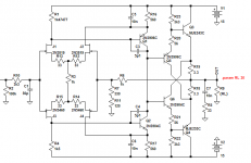
I spiced essentially the same circuit late last night but use 2SK117, which is essential identical to one half of a 2SK2145.
I use 750R for R3, and 1k for R4 & R5.
Closed loop bandwidth for gain of +2 and -1 are all over 10MHz.
Too much gain at HF. So need a Zobel somewhere.
Only first shot. Some way to go.
Need to get proper models from Toshiba.
Cheers,
Patrick
> Speaking now of the Constellation-like simplified schematic from JC's post #168:
I spiced essentially the same circuit late last night but use 2SK117, which is essential identical to one half of a 2SK2145.
I use 750R for R3, and 1k for R4 & R5.
Closed loop bandwidth for gain of +2 and -1 are all over 10MHz.
Too much gain at HF. So need a Zobel somewhere.
Only first shot. Some way to go.
Need to get proper models from Toshiba.
Cheers,
Patrick
Great.. what are your ideas?!
http://www.diyaudio.com/forums/anal...iscrete-opamp-open-design-14.html#post3140092
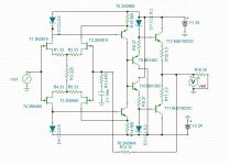
I'm on the Bonsai side (FET only in the input stage, please ), and I'm going to give a try in a few days to this little beast - it is basically a JC-2 with a high current diamond output stage suitable for driving low Z headphones: simulation results are quite good (OLBW > 30 kHz, THD < 0.001% up to 20 kHz @ 100 mW into 30 ohm), and employs fairly standard parts (it happens my drawers are full of 2N3819 and 2N5460 ) - I'll let you know.
Ciao,
L.
), and I'm going to give a try in a few days to this little beast - it is basically a JC-2 with a high current diamond output stage suitable for driving low Z headphones: simulation results are quite good (OLBW > 30 kHz, THD < 0.001% up to 20 kHz @ 100 mW into 30 ohm), and employs fairly standard parts (it happens my drawers are full of 2N3819 and 2N5460 ) - I'll let you know.Ciao,
L.
Attachments
Speaking now of the Constellation-like simplified schematic from JC's post #168:
....one of the problems is that the lower output device must supply all of the input bias current of the upper device, so this intrinsically unbalances the P pair. Throw down a current sink from the output (or just a resistor to the negative rail), then the second stage can be balanced. It's also good to put some voltage drop in the one drain to equalize the drain voltages of the P devices.
....
Now some can argue that the bias resistors could be made larger, but then we run the second stage at lower current, and the input capacitance of the lower N output will slow that section down.
At least, if the two output devices are reasonably well-matched, and perhaps with some ballasting R in the sources, the quiescent bias can be not too unstable.
The proposed source resistors at the output stage are essential for a rugged real life design. Fortunately we are not heading for efficacy and/or excessive output swing, we can easily spend 1V on each source resistor, which will knock down the thermal drift of the output stage reliably and avoids the need of further thermal compensation diodes and thermal couplings with the input stage.
Such source resistors will theoretically increase the output impedance, which is not so much desired, but good for PSRR . Bringing down the output impedance and keeping high PSRR can be done by a I/V resistor at the output (...was somewhere proposed earlier anyway), but most likely increases distortion compared to light load situations.
The intrinsic imbalance can also be reduced by giving the lower Mos a higher source resistor value.
I guess the original usage of that circuit was in an application were the output stage is running at significantly higher currents compared to the driving stage (ref. quasi complentary BJT output stages of power amps).
Regarding the 2nd order distortion struggle between Wavebourne and John, I tend to say that Wavebourne's concerns are basically fitting to the nature of the circuit. The tail which drives the upper output device is operating at massively modulated Vds while the tail which drives the lower output device is operating at low modulation of Vds. Anybody crying for cascoding? No, I would tend to live with it.
Last but not least. I doubt that a simulation with standard models is the right tool to analyze distortions in the sub -80db range.
In my experience the sim helps to find the right direction and see the fundamental nature of the distortions. But in all my past simulate+build trials it turned out that the sim was much nicer than reality.
I'm on the Bonsai side (FET only in the input stage, please
Ciao,
L.
Nice
I like the general structure, but why are C5 and C6 so high? I would MIC this op-Amp for high slew rate. There is the opportunity here to go with a single N chan FET LTP (easy to get) rather than the bfully alanced symmetrical.
I'm on the Bonsai side (FET only in the input stage, please
Ciao,
L.
This one gets my vote. It has 10 transistors though.
I'm on the Bonsai side (FET only in the input stage, please
Ciao,
L.
I juiced up the whole thing and distortion is now 0.0005% @ 20kHz into 30 ohms @ 1.1Vrms. DC offset on the output is -1mV.
I have since added Miller capacitors (@10pF each) to get rid of a 15dB spike @ 10MHz. Distortion is now 0.0006% under the above conditions. S/N is 120dB @ 10kHz.
Unfortunately, large heatsinks are required on the outputs.
Finally, something I understand.
Attachments
Last edited:
I juiced up the whole thing and distortion is now 0.0005% @ 20kHz into 30 ohms @ 1.1Vrms. DC offset on the output is -1mV.
I have since added Miller capacitors (@10pF each) to get rid of a 15dB spike @ 10MHz. Distortion is now 0.0006% under the above conditions. S/N is 120dB @ 10kHz.
how is dc output offset and drift again ?No coupling caps (10mfd) anywhere and no dc servo?
-RNM
Last edited:
- Home
- Source & Line
- Analog Line Level
- Discrete Opamp Open Design