Where is this thread please?
I see Mike is back. I have two weeks to a tapeout and then I should get time to rev my boards and take more measurements.
Hi Frank,
Does this go for the Intel/AMD chip and socket in your PC.
Perish the thought of ever using a valve in a socket !!

Which is why I would approach the concept of a valve amp very, very carefully ... things are very different in the latter world, lots of heat, temperature cycling is ferocious, chunky connectors, high voltages - like going from a chamber music performance to a disco, electrically speaking ...
Frank
Frank
I think I've found a test signal:
WALTER MURPHY- A Fifth of Beethoven (extended version) - YouTube
WALTER MURPHY- A Fifth of Beethoven (extended version) - YouTube
How so? Fairly straightforward mix of classical and light jazz acoustics, shouldn't be too hard ...
Now, if I want a decent stress test I would try some 90's Joe Cocker, "You Can Leave Your Hat On" era material: big, big acoustics, full on big band sound -- this is sound that can subjectively grab your house and threaten to crush it like a cardboard box if it's reproduced well at high volume ...
Frank
Scott's still on to it, but not a single other person has hacked one of these to see what they think of it ... ?
SWOPA is a bit too complicated for me, so I went with a Class-A folded Kaneda with 7 actives in 11mm x 14mm SMD. I've built over a dozen prototypes with slight tweaks and parts changes, and it's now stabilized with tight offsets.
I also did a Class-AB FET990 derivative in 15mm x 15mm, and the first batch of boards is in transit to me. These can use BF862 or 2sk209 inputs, and SOT89 outputs like the 2sa1213/2sc2873.
I also have an updated schematic and layout for the FET990 with jcx's clamp-diode bootstrap idea, also in 15mm x 15mm, but I'll hold off on fabrication those boards until the existing board is fully validated and auditioned.
I'm still searching (in simulation) for a simple topology with low transistor count and acceptably good performance. Nothing beats the FET990 derivatives to date.
For the output-stage, Ken Peter's non-switching Class-B with Schottkys is a very strong contender for low-bias current applications - it works reasonably well down to 1 mA bias and maybe lower. However, it does best with a high-performance monolithic opamp as the gain stage driving it.
Have you a link to this please.For the output-stage, Ken Peter's non-switching Class-B with Schottkys is a very strong contender for low-bias current applications - it works reasonably well down to 1 mA bias and maybe lower. However, it does best with a high-performance monolithic opamp as the gain stage driving it.
I'm going to risk sounding off as a audiophile who is not an EE, but why hasn't someone advocated an all npn Class A output stage. I thought that pnp transistors typically had much higher c-b capacitance which slows their switching speed for Class B-AB stages. I read that the Burr Brown OPA604 had an all npn output state. So why in a no holds barred design are we possessed with efficiency? Please be kind! Cordially, Ray
If your going to use Joe Cocker as a test use 1985's Shefield Steel with Sly and Robbie as the rhythm section. Not a commercial hit, but Joe doing great dynamic music instead of the commercially viable Musak he's been stuck with for decades.... Now back to our program
Last edited:
The aim is not to use recordings which are dynamic in their music content, rather those which are produced with certain engineering styles. Just had a quick listen to Sheffield Steel on YouTube, and it would not be a good contender for the type of testing I was thinking of - the engineering is too straightforward, wouldn't stress the system sufficiently ...
Edit: You need recordings that have everything, AND the kitchen sink to do this. Which reminds me, another excellent recording for such is the soundtrack for the film, "Moulin Rouge": this has a massive sound in many of the tracks, most systems would struggle to recreate what has been encoded at decent volumes ...
Edit: You need recordings that have everything, AND the kitchen sink to do this. Which reminds me, another excellent recording for such is the soundtrack for the film, "Moulin Rouge": this has a massive sound in many of the tracks, most systems would struggle to recreate what has been encoded at decent volumes ...
Last edited:
I don't think You Tube qualifies as a high quality source to judge much of anything - probably the best Shefield Steel track for dynamics is Ruby Lee, the Mobile Fidelity album or CD are nice transfers for the time, but you seem to have something else in mind - ah well back to the salt mines ......
Last edited:
No, YouTube won't give you the quality in direct replay but you can use it to assess the processes used in the studio, the level of complexity of the mix. Having said that, many music tracks on that website are available at high bit rate, and if you download them and resample to normal uncompressed digital people might get a shock as to how good they can sound ...
The "something else" I have in mind is to give my system a hard time, force it to work hard for its living, that way I know it's got the chops for all sorts of material. Put it this way: if you're going to buy a car would you test drive on the smoothest, straightest road you can find, or would you want to know how it handles itself on a rough back road?
The "something else" I have in mind is to give my system a hard time, force it to work hard for its living, that way I know it's got the chops for all sorts of material. Put it this way: if you're going to buy a car would you test drive on the smoothest, straightest road you can find, or would you want to know how it handles itself on a rough back road?
Back to the drawing board
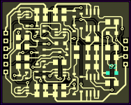
This is my own interpretation of Scott's masterpiece. Design criteria are:
- all SMD
- as small as possible but with reasonably sized components and spacings, must be hand-solderable for prototyping
- use of matched components where possible, without resorting to hard to find parts, all semis are from NXP and available through standard catalogue vendors like Digikey, Farnell, etc.
- diamond buffer is made of two complementary pairs in SO8
- current mirrors are integrated parts containing two matched BJTs
- diodes are diode connected BJTs for matching
- pinout includes gmC stage output, compensation pins, offset nulling, beside the usual ins, outs, Vccs
I'd like to hear some expert opinion on the layout of my small board. Specifically, I'd like to hear comments about manufacturability, and criticism on obvious mistakes I may have overlooked.
Thank you
Giorgio
Attachments
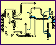
"manufacturability"I'd like to hear some expert opinion on the layout of my small board. Specifically, I'd like to hear comments about manufacturability, and criticism on obvious mistakes I may have overlooked..
Hi Giorgio,
Hard to say without knowing what exact parts (BOM) are used, there orientation referenced to the schematic, sizes of the pads etc.
Post the schematics, gerber/drill data and then I/someone can actual make any sense of a pcb with some lines drawn on it
Every pcb shop has their capabilities, so you first have to find a supplier & meet their guidelines.
If you keep (line/space) > 8mil(0.2mm) you are good to go for most fab's. I usually pick 12mil as default for signals and 25mil for power(For a small pcb as this). For vias I use (32V20) 32mil pad/20mil finished hole (batchpcb req.). If you need smaller then, 30V16,(8/8) 25V13(5/5). Your minimum pad pitch usually sets your minimum line width, a simple rule to follow. I have used a few DFN's (QFN40-6X6-LS0.5MM), I come off the pads with a 9mil trace and then wick up from there.
It is also good to use the widest trace and spacing as possible.
My acid test is always to print out the component mounting layer(s) (1:1) and physically place the comp on the footprint just to be 100% that I got it right.This means getting the components ahead of time or have mechanical equivalents to verify your new/unproven footprints. The quality of the CAD library is imperative or you are wasting money on bad pcb's. I never use the ones that come with the CAD package. From my experience, I find issues with them all, it is a long list of things to check for.
Where are you planning to get a pcb fab'd? Home or outsourced?
I have a few pcb to be made, was looking at
PCB prototype manufacturer doublesided and multilayer - PCB-POOL.COM
or
https://batchpcb.com/
Rick
Last edited:
Rick,
Thank you for your response.
Some more details:
- board size is 42 x 33 mm
- semis are SOT23 size and equivalents
- resistors are 1206
- signal traces are 0.33 mm / 13 mil
- power traces are 0.5 mm / 20 mil
- vias are 40 mil diameter / 20 mil hole
- PTH are 60 x 60 mil pad / 35 mil hole
- clearances are set to 6 mil minimum in DRC
Your suggestion about printing out the top layer and place components for a quick check is very good and I will definitely follow it as I'm using the standard CAD package libraries. I will check them out to see if they need improvements.
Also, PCB pool seems to exactly fit my needs.
Thank you
Regards
Giorgio
Giorgio,
Set your DRC rules for 8 mil spacings and see how many violations that you get?
SOT-23/1206 good choices, this is my preference as well for something like this, no need for 0805.
Your design is what I know as 12/12 technology, except your 6 mil DRC is too close for 12/12, so it is a mix. 8 mil DRC min spacing, is a safer way to go for a design such as this, your choice however. These days 5 mil spacing is a safe bet even for ? pcb shops.
I am always surprised how many EE's, can not or chose not, to layout there own pcb's. It is a very important part of the design process, just like software and mechanics.
Cheers
Rick
Rick,
DRC clearances set at 8 mil passes with no errors.
The default DRC setting for ground plane to board sides clearance is 25 mils and is clearly violated in my layout. I wonder whether this is really critical however. I could easily change either the clearance setting or the ground plane area but I'm not sure it is really worth it. Any suggestion?
I totally agree with you about layout being part of the design process. I'm doing this exercise because it is a great learning experience, beside for the fun of it.
Thank you
Regards
Giorgio
Last edited:
If you bring your copper to routed edge, then you will get burrs, as this is the last operation, routing the image out of the panel.
I am doing a design now, RF using a Si4770, I want the option of putting a shield around the whole pcb ( & ground it) , so this is the only reason why I will bring the copper to the very edge of the routed edge.
Yes layout is fun for me as well. Gives you the physical perspective, which is usually a paper design, up this point in the design cycle, unless you do some prototyping before doing final layout.
In so many designs, the pcb layout is a throw it over the wall approach, which is flawed in so many ways.
Rick
Last edited:
- Home
- Source & Line
- Analog Line Level
- Discrete Opamp Open Design