Hi Scott,
The information Ive seen showed improvement for extremely low distortion levels, like around -100db.
Takes the falling fb/response/phase shift associated with it out of the picture -->

(A.Sandman)
Takes the falling fb/response/phase shift associated with it out of the picture -->
View attachment 327400
(A.Sandman)
What does that have to do with cap load drive? Put some practical numbers up there for say an RL of 600 Ohms and net gain of 20dB. An amusing conceptual circuit but not practical in many cases. Do a noise analysis for instance, or if the summing resistances are much less than RL you get all the distortion back by shoving most of your current into the correction amp.
Last edited:
For those of us without EE degrees, it would be nice to know what is the external compensation (output back to minus input and the resistor to ground. IE values for R13 with C3 of 15pf in parallel and R6 on D5BB schematic) for 10db of gain, 20db of gain and 40db of gain. Thanks, Ray
Transistor selection
I'd like to go full SMD to avoid the somewhat complex assembly of TO92 devices in the output stage. OTOH, I'd like to retain the thermal tracking feature of the PTH configuration while driving low loads.
I've been looking for dual NPN/PNP transistors in SMD packages capable of some power dissipation and the only parts that I came up with are the NXP PBSS4041SPN:
http://www.nxp.com/documents/data_sheet/PBSS4041SPN.pdf
It seems to me that those parts are designed for (static) switching rather than linear operation. They are also comparatively slower than 2N4401 / 2N4403, for instance.
Questions for the Semiconductors Gurus:
- are those parts any suitable for the output diamond buffer?
- any similar, better, parts?
Thank you.
Giorgio
What does that have to do with cap load drive? Put some practical numbers up there for say an RL of 600 Ohms and net gain of 20dB. An amusing conceptual circuit but not practical in many cases. Do a noise analysis for instance, or if the summing resistances are much less than RL you get all the distortion back by shoving most of your current into the correction amp.
...cap feed back to output to lower distortion... just caught me funny and I had this zanny idea - image- that it was summing and canceling distortion but another opamp in place of a cap would be more complete... thus A.Sandman's circuit. Sorry, its just the way I think sometimes. Its like a flat rock skipping across the surface of water... one point of contact quickly leads to another and who knows where it will end.
BTW- the circuit was published in Wireless World and taken to a working circuit level... into 8 Ohms. Feb 1974. It has its applications and ought be perfected (in IC's?). Or in discrete?
Oh, never mind.... carry on....
Last edited:
It seems to me that those parts are designed for (static) switching rather than linear operation.
Giorgio
So were the 2N4401 and 2N4403. They wound up being very good for noise if the circuit impedances are low and you send enough current through them, especially the 4403; although once people started to pursue low base spreading resistance as a primary goal, the 4403 was superseded. But we didn't use enough of those so they were discontinued. The more things change...
But what the impact of the lower gain bandwidth will be for the parts in question, and in this application, I don't know, but I'd like to play with them.
Thanks for this Giorgio.I've been looking for dual NPN/PNP transistors in SMD packages capable of some power dissipation and the only parts that I came up with are the NXP PBSS4041SPN:
http://www.nxp.com/documents/data_sheet/PBSS4041SPN.pdf
Dunno about suitability for diamond output but they sure look interesting for Lo R Lo Noise.
If you believe their Vbe (sat?) 1.05V for Ib 400mA, that means rbb should be MUCH less than 1.05V/400mA = 2R65 !

I'd have a caveat about 1/f noise but this is certainly worth investigating.
Last edited:
...
BTW- the circuit was published in Wireless World and taken to a working circuit level... into 8 Ohms. Feb 1974. It has its applications and ought be perfected (in IC's?). Or in discrete?
Oh, never mind.... carry on....
As a unity gain inverter (does not work at all in follower mode) and an inverter with gain again presents a low impedance to drive, so the usefulness?
There are a host of footprints out there; The Deane Jensen 990, The Pacific Recorders 990, the John Hardy 990, the API2520 and DIP8. And what about FM Acoustics modules? I think there probably needs to be an adapter for each case. And in each case I don't think this is gona be plug and play...
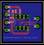
I don't know if this is a workable option, but here is a first-pass layout of an API2520 to DIP8 single-opamp adapter. Of course, the opamp will have to be chosen to be able to handle high rail voltages of +/- 24V if necessary, which limits the available choices (the alternative is to put two low-noise low-dropout +/- 15V regulators on the adapter board, but that opens up another can of worms about dirty/clean grounds, input signal clamps, etc.).
R1 may be a zero-ohm resistor, in which case the adapter ground-plane is directly hitched to the dirty ground, or it may be a lift resistor of a few ohms to isolate it from the dirty ground. The C1,C2 rail-to-ground bypasses are optional.
It should be possible in principle to use a DIP8 discrete (like the folded Kaneda I posted earlier) in place of a monolithic opamp with the adapter.
Attachments
Regarding your capacitor C2, is there a consensus about passing a trace between the legs of a part in 0805-package? As I recall, for quite a while the manufacturers said "Don't do that!" and the manufacturing engineers were solidly behind them - but circuit designers and PWB layout folks said, "Hey, it makes the routing easier and if production has their feces amalgamated the failure rate isn't enough to worry about.".. . here is a first-pass layout of an API2520 to DIP8 single-opamp adapter . . .
Are there any recent thoughts or statements about this?
Dale
Regarding your capacitor C2, is there a consensus about passing a trace between the legs of a part in 0805-package? As I recall, for quite a while the manufacturers said "Don't do that!" and the manufacturing engineers were solidly behind them - but circuit designers and PWB layout folks said, "Hey, it makes the routing easier and if production has their feces amalgamated the failure rate isn't enough to worry about.".
Are there any recent thoughts or statements about this?
Dale
It is still bad practice. The PCB trace going between the pads is covered by solder mask but the pads are not. Therefore, the 0805 component fails the coplanarity test i.e. it does not sit flat and rocks, end to end. What might seem acceptable to a diyer or a design engineer that only ever builds one unit, is not acceptable to production/manufacturing engineers who take responsibility for building hundreds and thousands of units.
What if one left the solder mask off the trace under the 0805 part?It is still bad practice. The PCB trace going between the pads is covered by solder mask but the pads are not. Therefore, the 0805 component fails the coplanarity test i.e. it does not sit flat and rocks, end to end. What might seem acceptable to a diyer or a design engineer that only ever builds one unit, is not acceptable to production/manufacturing engineers who take responsibility for building hundreds and thousands of units.
traces under 0805
Few options, first is to use a via, of course. Use a 1206 part. Also if/when they wave solder backside, they usually use glue to hold the component in place. Wave soldering will do a better job in this case rather than a paste & re-flow process.
Introduces other problems, if component is off center could cause a short, under the component (hard/impossible to see) or a possible place for a solder whisker to form.What if one left the solder mask off the trace under the 0805 part?
Few options, first is to use a via, of course. Use a 1206 part. Also if/when they wave solder backside, they usually use glue to hold the component in place. Wave soldering will do a better job in this case rather than a paste & re-flow process.
Last edited:
Introduces other problems, if component is off center could cause a short, under the component (hard/impossible to see) or a possible place for a solder whisker to form.
Few options, first is to use a via, of course. Use a 1206 part. Also if/when they wave solder backside, they usually use glue to hold the component in place. Wave soldering will do a better job in this case rather than a paste & re-flow process.
Well I can see that --- but based on the sort of contemporary geometries being used routinely, and the "huge" dimensions of an 0805, and the fact the the trace could be skinny in that vicinity... isn't that concern fairly minor?
Now if it is diy and I'm the one placing and soldering, I'd heartily agree
But as a general consideration for automated assembly I'm surprised it would still be a prohibition.Of course things have gone to H E double hockey sticks since ROHS...
The solder mask is typically 15-20um thick so if you specified 1oz copper weight (35um thickness) and pulled back the solder mask clear of that nasty traces you would be ok. But the copper will corrode. You will have a short shelf life for the PCB unless you store it carefully - a humidity cabinet is then required. So you then decide to plate the copper with a finish that does not itself corrode. So you go for ENIG (Immersion Gold over Electrolysis Nickel) - it looks pretty too although your PCB is now more expensive. And you need a silver bearing solder paste... which is more expensiveWhat if one left the solder mask off the trace under the 0805 part?
Or, you just NOT route that pesky trace under the 0805!
Also if/when they wave solder backside, they usually use glue to hold the component in place. Wave soldering will do a better job in this case rather than a paste & re-flow process.
It really depends on the assembly house. The 'backside' could be done using reflow with a higher temperature solder paste and then the 'frontside' is done with a lower temperature solder paste. Through-hole components (e.g.connectors) could use selective wave solder where a mask is used.
For something like this issue, the assembly house often just looks at the design, curses the bleeping designer and adds a surcharge to cover the rework and failure rate for this and other 'nice' layout features. It is only when the design is properly reviewed/redesigned that manufacturing and field failures 'magically' reduce.
- Home
- Source & Line
- Analog Line Level
- Discrete Opamp Open Design