I posted this a few months ago and someone was nice enough to decode all the colors, I lost track but it is here somewhere. One thing is obvious no sweeping generalizations about all SMT resistors apply.
Last edited:
We know which of the THole types are the better ones..noise AND THD; So i am going with that until i know which sm are the best or better than the th type.I posted this a few months ago and someone was nice enough to decode all the colors, I lost track but it is here somewhere. One thing is obvious no sweeping generalizations about all SMT resistors apply.
For example, the Dale metfilms th types are available everywhere and do very well at both noise and thd and are cheap to boot! I suspect the formulations used on th and sm are the same (?) and thus might go blindly for Dale with sm as well. Until shown other wise.
-Thx RNMarsh
Last edited:
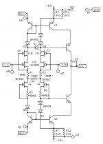
This is the input stage that I tested with the output stage I posted a week or so ago. Everything looked good, the distortion was hard to measure and the amp was stable well below a gain of 10, so I see no problems in proceeding. I have spent a lot of my personal time on this and will stop now.
Attachments
Retired SW-OPA
SW --- you said you could and then you would. And, now you did. Thank you for an enjoyable ride thru this. Well done. Learned a lot and had fun, too. Now the SW-OPA is a part of the universe/internet forever.
Soon you'll retire yourself as well. Then what, i wonder. Will there ever be a SW-OPA-2 in the furture? A sequel?") Thx, Scott - Dick Marsh
Thx, Scott - Dick Marsh
SW --- you said you could and then you would. And, now you did. Thank you for an enjoyable ride thru this. Well done. Learned a lot and had fun, too. Now the SW-OPA is a part of the universe/internet forever.
Soon you'll retire yourself as well. Then what, i wonder. Will there ever be a SW-OPA-2 in the furture? A sequel?
Thx, Scott - Dick Marsh
Last edited:
... I see no problems in proceeding. I have spent a lot of my personal time on this and will stop now.
Scott, great work and thanks for the contribution of your valuable time and energy to this project.
Hello Scott ,
In post 2591 :-
http://www.diyaudio.com/forums/anal...screte-opamp-open-design-260.html#post3322936
The hardware that you show is it designed to fit into a standard dip 8 footprint.
Regards
Arthur
In post 2591 :-
http://www.diyaudio.com/forums/anal...screte-opamp-open-design-260.html#post3322936
The hardware that you show is it designed to fit into a standard dip 8 footprint.
Regards
Arthur
Hello Scott ,
In post 2591 :-
http://www.diyaudio.com/forums/anal...screte-opamp-open-design-260.html#post3322936
The hardware that you show is it designed to fit into a standard dip 8 footprint.
Regards
Arthur
No that would take some work, I'm happy with 1"x1". You could probably make a tall doubleSIP style with two boards and have a DIP footprint.
EDIT - I'll continue to answer questions here and there, just the board layout and building is taking a little too much time away from other things.
Last edited:
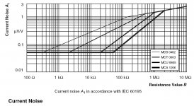
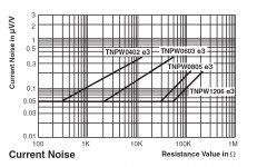
Concerning thin film resistor noise, I use these rules of thumb when doing parts selection.
0402 (or smaller): don't bother
0603 : ok up to 2k
0805 : ok up to 20k
1206 : anytime if space allows
Of course we still need to consider max. Pd, drift, max. voltage, tol. ...
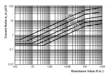
I cropped a few graphs useful to ilustrate the "size matters" aspect. The last one shows the thick films...in a class of their own
0402 (or smaller
): don't bother0603 : ok up to 2k
0805 : ok up to 20k
1206 : anytime if space allows
Of course we still need to consider max. Pd, drift, max. voltage, tol. ...
I cropped a few graphs useful to ilustrate the "size matters" aspect. The last one shows the thick films...in a class of their own
Attachments
Concerning thin film resistor noise, I use these rules of thumb when doing parts selection.
I cropped a few graphs useful to ilustrate the "size matters" aspect. The last one shows the thick films...in a class of their own
Interesting but there are counter examples of thick film on ceramic hybrid circuits of excellent performance or how about strain gages which operate at large DC currents.
Then there's IC thin film resistors orders of magnitude smaller where excess noise is nearly non-existant.
Indeed, I noticed that the Caddock MP9100 (100W, TO247) in the LIDO link is almost as good as a thin film. Tends to correlate with the last graph I posted where different sizes don't follow the same base line so at some point thick films will meet the thin films on noise performance.Interesting but there are counter examples of thick film on ceramic hybrid circuits of excellent performance....
Thin films in ICs...maybe there's a catch, but I wouldn't know
Interesting but there are counter examples of thick film on ceramic hybrid circuits of excellent performance or how about strain gages which operate at large DC currents.
Then there's IC thin film resistors orders of magnitude smaller where excess noise is nearly non-existant.
Research literature indicate that noise is higher due to thickness... sheet R. bulk. I suspect that not all "thin" films are as thin as others. IC thin films might be some of the thinnest. Thx-RNMarsh
Last edited:
Scott,
What is the recommended offset nulling scheme?
WRT the schematic of the input gain stage in your post #2643, a trimmer between the upper current mirror emitters (U1 emitter and W6 terminal) with the wiper connected to positive rail?
Also, is output current limiting necessary / advisable for the output buffer?
WRT the schematic in post #2593 a diode clamp (two anti-paralleled connected diodes) between output and the center tap of the 30K9 resistor to be split into two resistors?
Thank you (for the great learning experience)
Giorgio
Thanks very much for your considerable efforts and helpful tutoring.. . . I have spent a lot of my personal time on this and will stop now.
Dale
Revised Post #2620 Documentation
Post #2620:
The actual design shown here is the same as Post #2620! I will use the helpful comments (especially the information about surface mount resistors) to revise that design and create a new documentation package. I won't promise a delivery date for the next version.
ADDED COMMENTS:
3. Component Selection.
- A list of suggested component part numbers is presented in the Excel file "SW-OPA_Post2620_PL.xls". This file also includes suggested sources for each component, and their published retail prices. Most components show two suggested manufacturer's part numbers. The distinction between the "Preferred" and "Alternate" source is meaningless in this case - they could have been identified as simply "Choice 1" and "Choice 2".
4. Printed Wiring Board (PWB).
- There is provision to use either SOT23 or SOT223 devices in the output stage. Although pads are present for BOTH package types, an output device should be installed on only one set of pads.
-- The SOT223 mounting pads include an extended copper area serving as a heatsink. Based on guidelines published by NXP, the SOT223 devices mounted on this PWB would have a rated collector dissipation of 750 milliwatts.
- The three compensation capacitors are mounted on padstacks designed to accomodate several physical case styles: 0805 surface-mount components (e.g., Murata GRM series COG ceramic capacitors, or Panasonic ECH-U PPS film capacitors), 1210 surface-mount components (e.g., CDE MC series mica capacitors), or leaded components with 5 mm lead spacing (e.g., WIMA FKP2 polypropylene film capacitors, or CDE dipped mica capacitors in CD10 case size after minor lead forming).
- The drawing "Notes" call out a generic ROHS-compliant PWB. Modify as necessary for your situation and preferences.
-- For small-quantity, quick-turn PWB purchases the fabricator may offer a limited number of options, which may not include a fully ROHS-compliant board. You may, in fact, have little choice but to accept the materials, plating, finish, etc offered as the vendor's "standard" product.
-- Small-quantity purchases are usually negotiated via text files (easily modified to suit the situation) rather than formal drawings so the content of this drawing's "Notes" are unlikely to affect the transaction.
5. Gerber Files.
- I have included Gerber-format files that should be acceptable to many (perhaps the majority) of PWB fabricators.
- The files use the "RS-274X" format with embedded apertures so separate aperture files are not required.
- Dimensions are in inches and the numeric format is "4.4".
- Each file contains information describing the geometry of a particular "layer" of the PWB
-- A text file in the "Gerbers" directory identifies the layer associated with each file, and other details related to the fabrication. Many PWB fabricators require you to submit such a file with your Gerber files.
-- You must select, and perhaps do minor editing, of the particular files required by your PWB fabricator.
-- There are several no-cost Gerber viewer programs but I am not aware of any that offer editing capabilities. Several commercial programs - such as CAM350 and CAMtastic - offer time-limited evaluation versions that can do minor edits.
- The board outline is included on every layer as a 6 mil trace, as well as in a separate file containing ONLY the board outline.
-- A few fabricators want the board outline shown on each layer, and others will tolerate this practice.
-- Some fabricators want the board outline shown only on a particular layer - such as the top solder mask, top silkscreen, or even top copper layer. If your fabricator rigidly holds to such a requirement you will have to delete the outline from the other layers. (With even a rudimentary Gerber editor it takes only seconds to identify and delete the outline traces.)
-- Some fabricators want the board outline, and ONLY the board outline, shown in a separate file.
-- The center of the outline trace is the intended exact board edge. This seems to be the standard practice among PWB vendors but I can't guarantee that it is the universal method to interpret the outline traces. (Some may use the inner, or the outer, edge of the outline trace as the intended board edge.)
-- Many PWB fabricators require the Gerber files to follow particulat naming conventions. You may need to change the file names (especially the extension characters) before submitting the files.
- I included Gerber files for fabricating the stencil used to apply solder paste in an automated board assembly process. They are named "SWOPA2620PWB1.TSP" (topside solder paste) and "SWOPA2620PWB1.BSP" (bottom side solder paste). A hobbyist is very unlikely to use a paste stencil (they are expensive!) so these files should NOT be sent to the PWB fabricator, but they are included here to make the package complete. (Who knows? Maybe you'll decide to run off a batch of 500 of these things someday.)
Dale
Post #2620:
OK, here is the cleaned-up documentation, with Gerbers and a few other comments added. (See below.). . . - I intend to post revised documentation within 24 hours, including Gerber files that may be acceptable to some PWB fabrication houses.
The actual design shown here is the same as Post #2620! I will use the helpful comments (especially the information about surface mount resistors) to revise that design and create a new documentation package. I won't promise a delivery date for the next version.
ADDED COMMENTS:
3. Component Selection.
- A list of suggested component part numbers is presented in the Excel file "SW-OPA_Post2620_PL.xls". This file also includes suggested sources for each component, and their published retail prices. Most components show two suggested manufacturer's part numbers. The distinction between the "Preferred" and "Alternate" source is meaningless in this case - they could have been identified as simply "Choice 1" and "Choice 2".
4. Printed Wiring Board (PWB).
- There is provision to use either SOT23 or SOT223 devices in the output stage. Although pads are present for BOTH package types, an output device should be installed on only one set of pads.
-- The SOT223 mounting pads include an extended copper area serving as a heatsink. Based on guidelines published by NXP, the SOT223 devices mounted on this PWB would have a rated collector dissipation of 750 milliwatts.
- The three compensation capacitors are mounted on padstacks designed to accomodate several physical case styles: 0805 surface-mount components (e.g., Murata GRM series COG ceramic capacitors, or Panasonic ECH-U PPS film capacitors), 1210 surface-mount components (e.g., CDE MC series mica capacitors), or leaded components with 5 mm lead spacing (e.g., WIMA FKP2 polypropylene film capacitors, or CDE dipped mica capacitors in CD10 case size after minor lead forming).
- The drawing "Notes" call out a generic ROHS-compliant PWB. Modify as necessary for your situation and preferences.
-- For small-quantity, quick-turn PWB purchases the fabricator may offer a limited number of options, which may not include a fully ROHS-compliant board. You may, in fact, have little choice but to accept the materials, plating, finish, etc offered as the vendor's "standard" product.
-- Small-quantity purchases are usually negotiated via text files (easily modified to suit the situation) rather than formal drawings so the content of this drawing's "Notes" are unlikely to affect the transaction.
5. Gerber Files.
- I have included Gerber-format files that should be acceptable to many (perhaps the majority) of PWB fabricators.
- The files use the "RS-274X" format with embedded apertures so separate aperture files are not required.
- Dimensions are in inches and the numeric format is "4.4".
- Each file contains information describing the geometry of a particular "layer" of the PWB
-- A text file in the "Gerbers" directory identifies the layer associated with each file, and other details related to the fabrication. Many PWB fabricators require you to submit such a file with your Gerber files.
-- You must select, and perhaps do minor editing, of the particular files required by your PWB fabricator.
-- There are several no-cost Gerber viewer programs but I am not aware of any that offer editing capabilities. Several commercial programs - such as CAM350 and CAMtastic - offer time-limited evaluation versions that can do minor edits.
- The board outline is included on every layer as a 6 mil trace, as well as in a separate file containing ONLY the board outline.
-- A few fabricators want the board outline shown on each layer, and others will tolerate this practice.
-- Some fabricators want the board outline shown only on a particular layer - such as the top solder mask, top silkscreen, or even top copper layer. If your fabricator rigidly holds to such a requirement you will have to delete the outline from the other layers. (With even a rudimentary Gerber editor it takes only seconds to identify and delete the outline traces.)
-- Some fabricators want the board outline, and ONLY the board outline, shown in a separate file.
-- The center of the outline trace is the intended exact board edge. This seems to be the standard practice among PWB vendors but I can't guarantee that it is the universal method to interpret the outline traces. (Some may use the inner, or the outer, edge of the outline trace as the intended board edge.)
-- Many PWB fabricators require the Gerber files to follow particulat naming conventions. You may need to change the file names (especially the extension characters) before submitting the files.
- I included Gerber files for fabricating the stencil used to apply solder paste in an automated board assembly process. They are named "SWOPA2620PWB1.TSP" (topside solder paste) and "SWOPA2620PWB1.BSP" (bottom side solder paste). A hobbyist is very unlikely to use a paste stencil (they are expensive!) so these files should NOT be sent to the PWB fabricator, but they are included here to make the package complete. (Who knows? Maybe you'll decide to run off a batch of 500 of these things someday.)
Dale
Attachments
Thanks for that information! I was totally unaware of that problem. Several posts over the last couple of pages supported and expanded on your comments. I'll call out some other construction in the revised P/L.. . . I've seen horrendous excess (or so-called "current") noise in thick film parts.
Dale
You are correct that component spacing is very tight. Depending on your experience with SMT assemblies, and the soldering tools available to you, removal and replacement of individual components will be slightly, to extremely, challenging. On the other hand, the SMT implementation makes every circuit node accessible to 'scope or meter probes from one side of the board. My concept of "experimentation" is more along the lines of constructing an entire assembly to test an idea, especially since several components are likely to be changed as part of the experiment. At the other extreme, I know folks who think "optimizing" a design consists of trying every E96 value across an entire decade for each component location.. . . With the tight spacing of the parts as described, how will DIYer be able to access internal points to experiment?
To get the degree of accessibility you desire, can you suggest a suitable board size? Or, since I count 74 components in the parts list, what do you considerable a reasonable component density (parts per square inch)?
Dale
OK, I recall some discussion of SMT vs. thru-hole a few dozen pages back but I missed the requirement for thru-hole construction.zero, if all surface mount parts.
Thru-hole construction rules out use of the BF862 JFET (only available in SMT). What input device would be used? A pair of SK170's (as long as available . . . )? An LSK389 in the TO-71 can (assuming it can be purchased by mere mortals)?
A thru-hole version will necessarily require more acreage on the PWB. I count 161 pins distributed among 74 components. An old rule-of-thumb suggests 30 holes/sq inch as an upper limit in common PWB's (perhaps as much as 50 holes/sq inch in exceptional cases). Using the lower value a board area of almost 6 square inches would be required. Let's say 2.5" square, though I suspect it will have to be larger. Is that an acceptable size for a module like this?
Dale
Is there a consensus that Susumu "RG" series thin-film resistors are suitable in this design? They're about twice the cost of the common thick-film parts, and would add about US$2.00 to the BOM cost.Susumu seems to be the go-to brand for thin film in readily-accessible distribution.
Or should I be trying to find some other construction, such as a SMT metal film resistor?
Dale
- Home
- Source & Line
- Analog Line Level
- Discrete Opamp Open Design