Noise floor in the pictue looks strange, though. Are you using weighting filter?
Nope - just a quite conservative HF * input * filter: low level signals from my EMU are quite noisy, and at 60+ dB gain I just didn't want to turn the amp under test in a small LW tx
 . Output noise floor follows filter envelope, but level of the harmonics should be unaffected. I'm going to repeat the test during the weekend using the old faithful (HP 239A) as signal source - it's by far more clean in the HF range than my soundcard - I'll let you know. Have to understand why OL THD is lower (or CL THD higher) than expected.
L.
Last edited:
Obscure, here you go germanium JFET's at 4.2K.
http://ntrs.nasa.gov/archive/nasa/casi.ntrs.nasa.gov/20000031730_2000033912.pdf
Thank you Scott.
Fig.3 frequency scale looks a bit strange to me. Logarithmic, 3 decades, 8-188Hz.
Fig. 4 I think has been shown and discussed again.
It may lower noise, but lower temperatures definitely lowers conductivity of semiconductors, and at lower temperatures they just won't turn on.
Benb
I am really out of my waters here, but how lower “conductivity” matches with an increase in Drain current (fig. 2) and increase of transconductance (fig 4) of the above pdf?
George
At the time (when I was in college, late 1970's) I thought it was pretty useless information unless one was going to work in a transistor manufacturing plant, but now my opinion is one can't have too much knowledge.
So VERY true.
thermal couples
It seems that a lot of work went/goes into finding similar coeffecient of thermal expansion for semiconductor processes, materials and packaging.
As a practical note - the closer the two metals/materials are on the Periodic table, the lower the thermal electric effects.
But there are diffusion issues with solder alloys and metals... like gold easily diffuses into solder and makes the joint brittle. Et al. Tonnes written on such things. -RNM
(Just before the beer)
I am surprised.
First by the answer from the experts, as I think that this problem had to be addressed in microcircuits and micromachines.
Second by the “research” on copper/solder/copper. What research? This is the most common/dominating case of electrical connection in electronic circuits for how many decades?
It seems that a lot of work went/goes into finding similar coeffecient of thermal expansion for semiconductor processes, materials and packaging.
As a practical note - the closer the two metals/materials are on the Periodic table, the lower the thermal electric effects.
But there are diffusion issues with solder alloys and metals... like gold easily diffuses into solder and makes the joint brittle. Et al. Tonnes written on such things. -RNM
Last edited:
Thank you Scott.
Fig.3 frequency scale looks a bit strange to me. Logarithmic, 3 decades, 8-188Hz.
Fig. 4 I think has been shown and discussed again.
Benb
I am really out of my waters here, but how lower “conductivity” matches with an increase in Drain current (fig. 2) and increase of transconductance (fig 4) of the above pdf?
George
Lower temperature helps for a while with Silicon, but just not much colder than 100 K. The improvement is both as an increase in gm and a reduction in the temperature and thus thermal noise of the material. And if you are concerned about measuring tiny amounts of charge, the reduction in gate leakage is profound, provided the drain-gate voltage is low enough.
Germanium is a lot different than Silicon. GaAs also works pretty well at Helium temps.
One anecdote: low-temperature physicists did some circuitry that had to be very cold with bipolars. In order to have mobile carriers for transistor action, they included "grain-of-wheat" incandescents in the mix and had a little near-IR light shine on the chips. This I heard from Edward L. "Ned" Wright, a brilliant guy at UCLA. Eventually they got some devices made that worked without the light, by "doping the pee out of them"
Of course they didn't work very well at room temperature 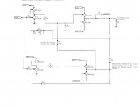
To clarify what is up in #766: Consider everything above R12 and R16. It's a fairly straightforward common-source amplifier with a matched current source load, with a floating level shift to a common-drain voltage follower with a matched current sink load. Closing the loop around it produces an inverting gain of about unity, with the noise dominated by resistor thermal noise. The performance by itself is not bad at all considering the minimal component count. The level shift could be done in a number of ways, perhaps the best except for physical size being a battery.
The stuff added to it enhances performance markedly, by effectively increasing loop gain and eliminating loading on the upper section's output. And yet the auxiliary section adds almost no noise --- the upper section remains by and large "in control".
The performance results will be spoiled to some extent by thermals in the input devices, since the full voltage swing appears there, although the BL parts should be close to a zero tempco operating point which will help a lot. There are ways around this with more parts. If the floating bias voltage in the upper section cannot be fairly low impedance, the helper resistor R16 can be capacitively coupled to the drain of Q1B.
Power supply rejection, distortion, and bandwidth predictions are all very good indeed. Nonfloating bias sources can be made but it adds a lot of parts. Variants include multiple output devices for higher drive current, higher-than-unity gain, etc.
No. Electron transport in a superconductor is significantly different than it is within semiconductors. The gap goop stuff was touched upon by benb.jneutron,
Very off topic, but if you take a super-conductor to very low temperatures it will stop the flow of electrons then? Just made me wonder your comment to George.
I did attempt to post a link, but it became very messy.(Just before the beer)
I am surprised.
First by the answer from the experts, as I think that this problem had to be addressed in microcircuits and micromachines.
Second by the “research” on copper/solder/copper. What research? This is the most common/dominating case of electrical connection in electronic circuits for how many decades?
George
I'll try again.
Here's the home page..
Lake Shore Cryotronics, Inc. is a Leader in developing innovative measurement and control solutions.
Yesterday I found reference information which included copper and solder joints. They didn't say much though, did provide techniques for making sure the joints didn't affect the measurement. I'll try again later.
Here's a helpful guide:
http://www.lakeshore.com/Documents/LSTC_appendixC_l.pdf
Here's calibration stuff.
http://www.lakeshore.com/Documents/LSTC_appendixD_l.pdf
jn
(Just before the beer)
I am surprised.
First by the answer from the experts, as I think that this problem had to be addressed in microcircuits and micromachines.
George
Sorry if I wasn't clear, I was looking into typical packages, a few microns of gold over kovar, and bond wires which are often alloys. I consulted an expert on the very thin metal film issues, in the end I concluded it didn't matter much by experiment.
Patents can be tricky things -- a current source where before there was a resistor and a jFET where there was a bipolar. Small things sometimes but in a competitive market it can help. For me it is the concept that counts - but knowing that the results are in the details.
I published the same bias topology with an all bipolar compl-push-pull line stage in the quarterly, TAA (3/80).
[The work, of course was done long before it got around to publishing.]
Pioneer never called me when I published my circuit maybe because it would put their patent in question as obvious appl of existing design. Note: Pioneer applied for thier patent same year (1980). And, granted in 1982. Certainly the circuit details are different (allowing a patent) but the bias topology had been done before their patent.
PS -- many of you know that when you work for a university or government - all inventions belong to them. One invention was a circuit topology for a MC pre-preamp appl. I got release from the Lab's patent lawyers to patent it myself... it had no use to their work so didnt want to pay for the patent -- I published it instead. What do I need a patent for that i should spend 10 grand to get it? And, I liked my day job. - Dick Marsh
One can say the same for the circuit you published in TAA, JLH published the original idea back in 1968 although he did use resistors and not ccs.
One can say the same for the circuit you published in TAA, JLH published the original idea back in 1968 although he did use resistors and not ccs.
JLH didnt invent that biasing form nor feedback scheme either... used in tube circuits long, long before then. I was just pointing out that the bias scheme was used by myself earlier than was noted ... not that I invented it. I was applying it to a different topology.
[If you dont understand the significant differences of the two topologies, there are plenty of books about the circuit and how it would differe from JLH design. One is: Emerging Techniques for High Freq BJT Amplifier design: A Current-Mode Perspective (1994) by C.Toumazou, J.Lidgey, A.Payne. Covers it so well, its in my reference library I keep. [ International Conference on Electronics Circuits and Systems, Cairo, Egypt.] But there are more contemporary books. -RNM
Last edited:
Here's a helpful guide:
http://www.lakeshore.com/Documents/LSTC_appendixC_l.pdf
Here's calibration stuff.
jn
This one helped me undertand the “thermal anchoring”. Very useful concept.
Talking about heat transfer, here is the useless information of the day
The solder/copper interfacial thermal resistance (ITR) is on average about 0.020 K·cm2· W−1.
International Journal of Thermophysics, Volume 26, Number 5 - SpringerLink
I am googling myself on the copper/solder thermo EMF but I can’t find any numbers yet.
George
This one helped me undertand the “thermal anchoring”. Very useful concept.
Talking about heat transfer, here is the useless information of the day
International Journal of Thermophysics, Volume 26, Number 5 - SpringerLink
I am googling myself on the copper/solder thermo EMF but I can’t find any numbers yet.
George
Thanks for the link, interesting read. the number, if they did it correctly, is certainly a useful one.
I must note:
1. They clearly don't solder for a living. They had to use a SAM to figure out they had voids??? Duh... Without weep or blow holes to clear flux and outgassing, what did they expect???
2. They consider the solder to copper interface as one entity? They don't realize that it is comprised of three layers? Two copper/tin intermetallic layers and then a pure solder layer lightly lead rich due to tin loss to the intermetallic formation??
3. Bet they didn't test the surfaces for solderability. They've probably no idea what percentage of the surface of the copper passivated with no metallic connection.
4. Their test technique is great when the thermal interface material is an order of magitude (or more) higher in thermal resistance than copper, as it produces a more isothermal secondary plate response. High conductivity interfaces such as solders tend to cause surface gradients on the secondary plate, remember it's a bounded geometry with edge causing specific heat discontinuty.
Soldering is a TWO THOUSAND year old technology. Still, mistakes are made..sigh.
I loved this gem:
""The density values were obtained by the
Archimedes’ method.""
No, tell me it ain't so. They displaced water to find the volume to calculate density? They used a rectangular cylinder of a known thickness, diameter, and weight, and couldn't calculate it's volume???? Shirley they jest...
But fun read. I would have checked the box "suitable for publication with revision".
jn
Soldering is a TWO THOUSAND year old technology. Still, mistakes are made..sigh.
LHC
Soldering is a process of alloying metals. Might find more info of your interest via Googling on alloying.
Yup. There's lots out there. I was tempted to google to get the copper tin ratios, but decided it wasn't worth it.
For tin/lead, the web has lots. For tin/silver, it's not as good out there as in house..
Problem with the web, is most do not have the understanding to be able to discern basic problems with what was written..the article linked being a good case in point. Most people won't even understand what I wrote, nevermind have the theoretical and practical underpinnings to figure out the article errors.
jn
R...I may have assumed incorrectly that you were speaking to me...if so....nevermind....
Last edited:
You got that right. They were TAUGHT about 15 years ago. I'd like to say ""did they listen...nooooo"", but that would be a cheap shot.. Personnel turnaround there played a large role in the explosion..those who were taught were not the ones who did. The information given them did not transfer during the personnel shuffles.
jn
It seems to me -- as a bonified old geezer now -- from hindsight - or the view from the bridge of my nose --> There is a lot of attention paid when something is new.... then it becomes mainstream. then it becomes forgotten. Then finally, lost -- in that order. Today new to forgotten happens a lot faster when the new gets folded into sim software. After that the derivation et al is forgotten.. and then lost. -Dick
Last edited:
I must note:
1
2.
3.
4.
I loved this gem:
But fun read
jn
Jeez, I only had access to the “Abstracts”

I’ll never confess to you the story of my life. You’ll nail me in a minute with a thousand nails
Problem with the web, is most do not have the understanding to be able to discern basic problems with what was written.
True but this may be the case with books too. The difference is that through the web we (I) have easy untargeted access.
Most people won't even understand what I wrote
Yes. And then here I come asking, putting you into the trouble to answer and kindly explain.

nevermind have the theoretical and practical underpinnings to figure out the …
Since many years now I have happily accepted the fact that I know very few things. And I try to read new. This I enjoy a lot.
My embarrassment comes from finding out frequently, that the things I know, I have understood them wrong.
But in general, I try to think positive
Ian Dury - Hit Me With Your Rhythm Stick [Official Video] - YouTube
those who were taught were not the ones who did. The information given them did not transfer during the personnel shuffles.
jn
In aviation industry there is a "politically correct" masquerading heading for this kind of messy issues: Human Factors.
For many years now it has become a mandatory training for the licensed engineers. Most of the curriculum is based on the aftermaths of such stupid common everyday mistakes.
George
Thermal-electric effects in metals
Google for Seebeck effect; The Seebeck coefficient is a material property that depends on temperature (micro volts/ degree C.) From that, EMF can be found....
Some Seebeck coefficients are: copper to silver or gold = 0.5 uv/C; Copper - nickel = 10; Copper to KOVAR = 40.
Strange one is copper to copper is not = 0 [thermal gradients matter].
Also google Thermal EMF of Solders.
Last edited:
- Home
- Source & Line
- Analog Line Level
- Discrete Opamp Open Design