Do good compliments exist?
What is the short list of good complimentary jFETs??
Thx - RNM
> This is not correct: 2x2SK117=2x2SK209=2SK2145=2SK3320
Was a typo from me in a rush. Sorry for my blunder.
2SK117 = 2SK209 = 2SK880 = 1/2*2SK2145 = 1/2*2SK3320
2SK246 = 2SK208 = 2SK879
2SJ103 = 2SJ106
Patrick
What is the short list of good complimentary jFETs??
Thx - RNM
Wavebourn, do you mean by that circuit similar to Widlar Op-Amp Current Source?
I am not familiar with such terminology. I mean, recording head should be driven my current source, not voltage source.
Id set at the zero temp - they work fairly well.
From the datasheet that's about 500uA. With 1K between the sources you would only have an average of .25V Vgs, so you can't use a lot of the distribution.
I'd say there are about ... none. The only P channel devices still in production that I know of are from two rather-low-performance processes, that from which the 5460 is drawn, and that from which the 5114 is pulled. Low gm, highish noise, low breakdown voltages.What is the short list of good complimentary jFETs??
Thx - RNM
There is of course stock here and there of the 2SJ74, the nominal complement to the 2SK170, and the even rarer P channel dual the 2SJ109 (complement to the discontinued 2SK389 dual). And at that the complementarity was focused on the transconductance, at the expense of capacitances and undoubtedly an even more extravagant die area. It is no surprise that Toshiba found them unprofitable to maintain.
On the other hand, partly because of the Benjamin Franklin direction of current flow
") there continues to be substantial development and availability of P channel DMOS with a reasonable range of properties. As remarked, there are no guarantees on noise, particularly at low frequencies, so in general such parts and their N channel cousins are not recommended for low noise early stages where the noise gain is high. As cascoding parts however, since the preceding transistor is usually possessed of a fairly high output Z, they can function reasonably well, except for the requirement of a gate bias for the enhancement-mode devices. Since the d.c. current at the DMOS gate is negligible this bias source can be a photovoltaic one or a battery, although this will hardly be very compact. I'm not sure if there are any depletion-mode PMOS devices like the NMOS DN2450 and similar parts, although if one were to order a million pieces maybe Supertex could be persuaded to try to make them
there continues to be substantial development and availability of P channel DMOS with a reasonable range of properties. As remarked, there are no guarantees on noise, particularly at low frequencies, so in general such parts and their N channel cousins are not recommended for low noise early stages where the noise gain is high. As cascoding parts however, since the preceding transistor is usually possessed of a fairly high output Z, they can function reasonably well, except for the requirement of a gate bias for the enhancement-mode devices. Since the d.c. current at the DMOS gate is negligible this bias source can be a photovoltaic one or a battery, although this will hardly be very compact. I'm not sure if there are any depletion-mode PMOS devices like the NMOS DN2450 and similar parts, although if one were to order a million pieces maybe Supertex could be persuaded to try to make them EDIT: Of course a folded cascode gets rid of the PMOS biasing voltage problem, but the pullup resistor that supplies current to the input device and the PMOS device has to be large enough to make the voltage noise of the PMOS have a small effect. This costs voltage and power dissipation. The resistor can be replaced with a current source, although still some volts are needed and the noise contribution from that source will be more than that of a resistor spanning the same available voltage.
Last edited:
From the datasheet that's about 500uA. With 1K between the sources you would only have an average of .25V Vgs, so you can't use a lot of the distribution.
Sorry Dick I misread the schematic (I read 51.1 Ohms on the penciled in values), you were aiming at 800uA but does not look too close.
Attachments
I'd say there are about ... none. The only P channel devices still in production that I know of are from two rather-low-performance processes, that from which the 5460 is drawn, and that from which the 5114 is pulled. Low gm, highish noise, low breakdown voltages.
The Fairchild PFET's are 'very' noisey.
Indeed --- I used to wonder if the old databook values could possibly be that bad. Unfortunately, they appear to be about right. Ouch!The Fairchild PFET's are 'very' noisey.
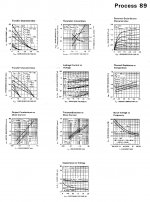
The attached is from an ancient National Semi databook, and the process 89 is from which the 2N5460-61-62 parts are sourced. The somewhat larger die from Process 88 is a good deal better, but both fall woefully short of the noise performance predicted by Van der Ziel, even at 100kHz, where the curves are beginning to level off.
In light of this, the 2SJ74 etc. was quite an achievement.
Attachments
The other problem here is that the complementary series connection ideally has both JFETs operating close to their zero tempco points. But it's work just to find that point for a single FET. When we need to do it for two of them AND have that operating point be the same magnitude, the selection task is daunting. Separate current generators could be provided I suppose, and the signals combined afterwards. But despite the appeal of a push-pull stage, a single-ended one has a lot going for it, particularly as good NFET duals still exist (and can be configured successfully as low-drift single-ended stages, or of course as conventional differential pair front ends).Sorry Dick I misread the schematic (I read 51.1 Ohms on the penciled in values), you were aiming at 800uA but does not look too close.
If we get lucky and the two track, that's another way that the phenomena can be saved. We still have high noise to deal with for the few currently-manufactured devices. With modest gains needed for some applications, perhaps the noise upstream will dominate, and of course the lower gains reduce the voltage drift concerns as well.
Only bad about it is:
The largest problem with the topology is finding good complimentary jFETs.. The noise of the ones I used here would only be good for line level work. But some jFETs designed for MC phono cartridges work well also. Selecting is the problem but it isnt hard nor expensive as the parts here were chosen to be easy to get and cheap as dirt. Others have tried the low noise compliments and get equally impressive results and still stable - dc-wise.
Originally I did it back in the late 70's with all bipolar, cascoded, current ourced et al. (published in TAA) Works fine too as it is easier to get good results and low noise etc. I just did it with jFEt's becuase they have been in vogue.
I am not sure the thermal stability is all attributed to the input, however.
the topology helps out some.
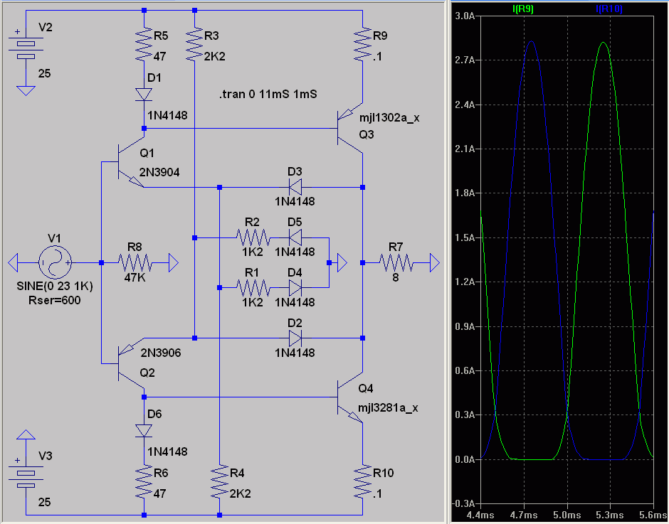
I ran the output pairs in equal currents per device and opposing with same re and havent sim'ed it but some distortion cancelling is evident..... both pairs used in push-pull helps reduce output stage distortion. Running at 45mA per output transistor. Linear output stage is more important when not using high gnfb design.
A biploar version was done originally, predecessor to current-mode opamp and is still very quiet and very low distortion. used a now obsolete Motorola quad of complimentary bipolars. Its hard to make great circuits and harder when the devices keep being obsoleted.
The differentail pair is a lot more practicle for most designs. matched same type is easy to find. One advantage of push-pull input is that the devices are in parallel instead of series (diff pair). but if you cant get the devices, the potential is lost.
BTW -- when I did my phono stage years ago.... it used two differntials and push-pull output. the input used 2N5564 pair that the data sheet said was 50nV/ but I had measured it to be 5nv/. I just looked it up... obsolete but -5565 still made... it is speced at 5nv now at low end and it is 1nV at mid-high audio freqs. So why cant the mfrer get this stuff right the first time? we still cant trust values used in SPICE for devices and still have to measure them oursleves. Shame on semi industry.
Thanks for the feedback and the conversations. I hope others reading of this forum got something out of it. Including the thermal issues discussed -Dick Marsh
The largest problem with the topology is finding good complimentary jFETs.. The noise of the ones I used here would only be good for line level work. But some jFETs designed for MC phono cartridges work well also. Selecting is the problem but it isnt hard nor expensive as the parts here were chosen to be easy to get and cheap as dirt. Others have tried the low noise compliments and get equally impressive results and still stable - dc-wise.
Originally I did it back in the late 70's with all bipolar, cascoded, current ourced et al. (published in TAA) Works fine too as it is easier to get good results and low noise etc. I just did it with jFEt's becuase they have been in vogue.
I am not sure the thermal stability is all attributed to the input, however.
the topology helps out some.
I ran the output pairs in equal currents per device and opposing with same re and havent sim'ed it but some distortion cancelling is evident..... both pairs used in push-pull helps reduce output stage distortion. Running at 45mA per output transistor. Linear output stage is more important when not using high gnfb design.
A biploar version was done originally, predecessor to current-mode opamp and is still very quiet and very low distortion. used a now obsolete Motorola quad of complimentary bipolars. Its hard to make great circuits and harder when the devices keep being obsoleted.
The differentail pair is a lot more practicle for most designs. matched same type is easy to find. One advantage of push-pull input is that the devices are in parallel instead of series (diff pair). but if you cant get the devices, the potential is lost.
BTW -- when I did my phono stage years ago.... it used two differntials and push-pull output. the input used 2N5564 pair that the data sheet said was 50nV/ but I had measured it to be 5nv/. I just looked it up... obsolete but -5565 still made... it is speced at 5nv now at low end and it is 1nV at mid-high audio freqs. So why cant the mfrer get this stuff right the first time? we still cant trust values used in SPICE for devices and still have to measure them oursleves. Shame on semi industry.
Thanks for the feedback and the conversations. I hope others reading of this forum got something out of it. Including the thermal issues discussed -Dick Marsh
Last edited:
Further note on the 2SK2145
I ran the voltage follower configuration I've been testing with the current generator connected floating gate (through a capacitor to the "source"), hoping to get some additional transconductance and hence potentially better drive capability and lower voltage noise out of it.
The drain-gate leakage is so low that the gate sits at only about a 65mV forward bias in this condition! But it did improve transconductance a bit, although as we know the noise is a weak (1/4 power) function of the drain current.
I really like these duals.
I'm about to post a somewhat whimsical circuit using floating bias sources and 2SK2145 devices, an inverting-only opamp at first. Please do not take it too seriously, although review may suggest some techniques to use elsewhere.
First,
jn
First, the most important issues:
I miss my mind the most..
Please, don’t shoot yourself.
It is obvious that your mind is in order . Appreciate what you have.
(*)The working speed of your mind when you were younger was the same as the speed it has now.
Your nostalgia is for the way your mind worked then, the working mode.
Now, many restrains (“what if”, “I know where this is going to end” e.c.t.) have unconsiously entered into the working equation. The thrust, simplicity, freshness and may be naivety of the youth have gone and give way to other attributes. The cumulative effect of “experience”.
I too miss my youth’s naivety but I try hard to expose any remains of it.
It's amazing what you miss when it is unavailable to you.
At the end of a week with no food (only nutritious intravenous injection) I started having illusions. The mirage was black olives and slices of bread flying over my head. I was tempted to raise my hands to reach them.
Your thinking is flawed only in that…
With the model you are proposing, I am afraid our thoughts will never meet. There has to be a capacitor (at least one) in the model, for the element of time (rate of heat transfer) to be addressed.
George
(*) It is also obvious that you have never really lost control of your mind. I wish from my heart that you or your beloved ones will never experience this.
looking forward to your schematics Brad. I checked the reel those parts came off of and they are listed as the Y classification diffused and assembled in Japan.
I hope they continue making them and add a P also!
Thanks again for those Wayne. I am also to receive some BL bracketed ones soon. Of course there is a limit as to how much current makes sense, since the dissipation is quite limited. However, based on my location of the chips in proximity to the gate leads, there is some hope that those leads will constitute some low-thermal-resistance places to remove heat, as is the case with most SOT-23 single JFETs. The easiest thing is just to provide a larger area of copper on a board, which isn't too painful if the gate is at a low impedance in the circuit. If it is not there may be other ways.
Although I've remarked that a little bit of elevated temperature isn't all that bad for thermal noise, in the case of JFETs the dissipation is also raising the resistivity of the material, so as to be something of a double whammy.
Since Toshiba has committed us to the two channels being hardwired together, the strategy of cascoding for any configuration other than a differential pair is denied. But I'm still cheered by what versatility is available.
I just did it with jFEt's becuase they have been in vogue.
As good a reason as any.
Here is one more topology that can be used in custom discrete opamp as an output stage. Actually, it is complementary symmetric opamp with 100% feedback. As drawn, it works in class AB, but output devices do not go through cut-off. If to remove diode-resistor shortening networks in tails and decrease values of resistors in tails it works in class A.
Diodes in current mirrors can be replaced by transistors. But not diodes in right sides of diffpairs: transistors have low base-emitter breakdown voltage, and when the amp goes from voltage follower mode to current amplifier mode (shortened output, or too low load impedance) transistors would be fried.
Resistors in tails instead of current sources are there on purpose: max current depends on output signal level.
> in the case of JFETs the dissipation is also
> raising the resistivity of the material,
So jfets have a positive temperature coefficient
like lateral mosfets ?
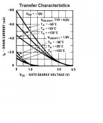
JFET's have two temperature coefficients the Idss and the Vp are opposite in sign so there is a point of zero TC.
- Home
- Source & Line
- Analog Line Level
- Discrete Opamp Open Design