Bcarso, I think you will find that the actual voltage noise derived from Gm is Re/2. The derivation is not obvious, but at least it does track Gm.
Isn't that what I said? If not, I wasn't being clear. I refer to it colloquially as a "half-thermal" noise.
To put some numbers to the remark about adequate collector current, with the voltage noise from the collector current shot noise, for one of the amazingly low rbb' parts like the 2SA1316 (~2 ohms), for the shot noise contribution to be the same as the thermal in 2 ohms, you need to run about 6.5mA. But if the beta is 500, the shot noise in the 13uA base current (the minimum noise ---usually it is rather higher than that, particularly at low frequencies) is about 2pA/sqrtHz. So the net voltage noise would be about 257pV/sqrtHz, and you will have again that much noise with the 2pA and a 126 ohm impedance source. So low impedance sources are indicated. I saw one stage run at about 125uA but using some of the low rbb' parts. The two devices were effectively in parallel so if similar their e sub n would be about 930pV/sqrtHz. That's low, but rbb' for each device could be a lot higher before you would see much of an effect.
Last edited:
> I already apologized for the typo.
Ninguna problema.
And I apologize for the ignorance.
> I meant 47 Ohm, but if to consider
> non - zero emitter resistance and
> non - infinite beta 26 Ohm indeed
> would be closer.
O.K.
> But input resistance will be no higher
> than 10K, so of course you can't
> substitute directly in all cases.
If I had a 470 Ohm emitter resistor,
and hfe of 100, wouldn't input
resistance be 47 k ?
George if you diagram it using (I know over simplified) the circuit analogy of input power as current, ThetaJ as a resistance, and temperature as voltage, you will see the point. Raising ambient ("ground") does not change the delta V's anywhere.
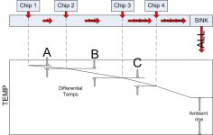
Here's a rudimentary semi-1D drawing. I have 4 chips, each dissipating equally. I put the dissipation exactly at the center of each chip for simplicity.
The sink is on the right, so all the heat flux must go towards it. While doing so, it causes a temperature rise in the substrate.
Note the differential A, it is the rise caused by chip 1 heat flowing towards the sink. B is the rise caused by the sum of chip 1 and 2 heat. C is of course, chip 1,2,and 3 causing the rise.
Note that the ambient rise is on the far right. The chip to chip rise is determined entirely by the power dissipated by each chip and the thermal conductivity of the substrate. If the substrate conductivity is not temperature dependent, then the rise chip to chip will remain independent of the ambient to sink rise.
Note also, the slope of the line between chips is proportional to the power flow. B is a large drop simply because it is a longer one. I made sure the slopes of the temp were correct with respect to the power total in the region.
jn
Attachments
Last edited:
Before we get too confused about a lot of things, let's put things in order.
First, if you have an active load, you should try to reduce the intrinsic (noise) gain of the load by reducing Gm through any means available, usually a series R.
You have to look at the whole input device assortment to determine how much FORWARD gain you will have. It is NOT the NOMINAL voltage gain, but the effective Gm(R[load]) where R[load] will be a very high and almost undefined impedance.
So since both the active load and the input see R[load] then the only thing you have to compare is their intrinsic voltage gain, each one, and the self noise of the active parts.
The 'trick' is to lower the Gm of the active load, to be lower than the effective forward Gm, in each leg, of the source.
This is NOT as easy as it might look.
To intuit the process, think about a SUMMING amplifier, where you have 2 separate active sources contributing. IF you do not use enough emitter or source resistor degeneration, you WILL not achieve what the input stage, itself, is capable of.
I was SHOCKED, shocked I tell you, when R.G. Meyer handed out a complete Spice analysis of the uA741, and SHOWED that it could have been quieter, except for the active load, in 1971.
Those with a sophisticated Spice program with separate noise contributions shown in a given design, would give further insight.
I have hilted in red the salient point we disagree on. The local delta T will not increase as the entire widgit increases in temperature.
The local delta T will be dependent on the heat flow between the components of interest, not on the absolute temp. As I pointed out, if the thermal conductivity between the local chips changes as a result of absolute temperature, so will the delta T between them.
I believe bcarso and I are agreeing, and we think differently from you.
Perhaps when I get the time, I could draw it up, verbal descriptions are not easy to express nor follow at times.
cheers, jn
It's like a voltage difference across a resistor. If you increase the voltage on both sides by, say, 100V, the current through the resistor doesn't change.
jan
It's like a voltage difference across a resistor. If you increase the voltage on both sides by, say, 100V, the current through the resistor doesn't change.
jan
Exactly.
The big problem with thermal however, is the heat capacity.....it makes objects act like a "capacitor", while long lengths can act like "inductances".
Another problem is how a substrate or pc is heatsunk. If the thermal conduction to the sink is low, the entire substrate will act as an isothermal island and it will take a long time to stabilize.
On a single chip, the issue not as bad given the distances involved.
jn
The big problem with thermal however, is the heat capacity.....it makes objects act like a "capacitor", while long lengths can act like "inductances".
We added device temperature as an independent variable to our simulator long before it was common. Another problem turns out to be that heat flow uses diffusion equations and the RC models are only an approximation. There is a wonderful paper on IC thermals by Billotti (sp?) deriving the relationships mathematically, the rule of thumb we use is about 15dB/die thickness which I remember as the heat goes in one face and comes out the other 5. It was amazing how close the intuitive answer was to the result of all the equations.
Last edited:
Isn't that what I said? If not, I wasn't being clear. I refer to it colloquially as a "half-thermal" noise.
If you consider the noise as comming from the collector current shot noise, the answer falls out.
cheers, jn
I have hilted in red the salient point we disagree on.
Better red than dead with this one

We certainly agree.The local delta T will be dependent on the heat flow between the components of interest
not on the absolute temp.
This is the #*@!$ point on which we dissagree.
In a nutshell: Doesn’t the Newton’s Law of cooling apply?
(“The rate of a heat loss of a body is proportional to the temperature difference between the body and it’s surrounding”)
Jneutron, Scott, Jan
Thank you very much for your time and effort. I appreciate.
But I still don’t feel I can agree to this.
It is not only that I am thick. I guess I have not managed to make clear what I mean too.
I really would love to have this discussion in a bar with a few beers and drawing some lines on a hand towel (and paying the round if I am wrong) but I have to live with typing characters.
I will try to visualize:
Scenario:
Transistor a and Transistor b of same small volume and composition, distance x=200um apart, encased in a big mass of silicon (IC chip).
Current has flown through a and b and has increased their temperature.
At time t0=0 current stops flowing. Trans a has temp Ta=100 C and Trans b Tb=70 C.
At time t1=10ms I would like to compare the deltaT between a and b (deltaTab) in two different cases:
Case 1: Silicon mass temperature at t0: Ts0=20C
Case 2: Silicon mass temperature at t0: Ts0=40C
I think (intuitively) that Case’s 2 deltaTab will be larger than Case’s 1
If you will tell me that I am wrong, this time I will accept it. Promise!
George
If you use regulated, very low z, low noise power supplies, what is the minimum psrr needed to not be an audible issue? [using topologies being discussed here].
Thx,
RNM
I think you can approximate that. If your output signal is a nominal 1V and you want -80dB S/N then whatever the power supply adds to the output should be below 100uV. Assuming the power supply has 1mV noise and ripple, 20dB PSRR would do.
jan
In your example, you have set the base of the silicon at two different temperatures, so to get the init temps you desire, 100 and 70 will require completely different power dissipations.Better red than dead with this one
We certainly agree.
This is the #*@!$ point on which we dissagree.
In a nutshell: Doesn’t the Newton’s Law of cooling apply?
(“The rate of a heat loss of a body is proportional to the temperature difference between the body and it’s surrounding”)
Jneutron, Scott, Jan
Thank you very much for your time and effort. I appreciate.
But I still don’t feel I can agree to this.
It is not only that I am thick. I guess I have not managed to make clear what I mean too.
I really would love to have this discussion in a bar with a few beers and drawing some lines on a hand towel (and paying the round if I am wrong) but I have to live with typing characters.
I will try to visualize:
Scenario:
Transistor a and Transistor b of same small volume and composition, distance x=200um apart, encased in a big mass of silicon (IC chip).
Current has flown through a and b and has increased their temperature.
At time t0=0 current stops flowing. Trans a has temp Ta=100 C and Trans b Tb=70 C.
At time t1=10ms I would like to compare the deltaT between a and b (deltaTab) in two different cases:
Case 1: Silicon mass temperature at t0: Ts0=20C
Case 2: Silicon mass temperature at t0: Ts0=40C
I think (intuitively) that Case’s 2 deltaTab will be larger than Case’s 1
If you will tell me that I am wrong, this time I will accept it. Promise!
George
In case 1, you are getting 80 rise in one, 50 rise in the second...power scaled is 8 to 5...
In case 2, you are getting 60 rise in one, 30 in the second. Power scaled 2 to 1.
The cases are different because the powers are different.
jn
ps..wish I could drink beer......I miss beer...
Better red than dead with this one
We certainly agree.
This is the #*@!$ point on which we dissagree.
In a nutshell: Doesn’t the Newton’s Law of cooling apply?
(“The rate of a heat loss of a body is proportional to the temperature difference between the body and it’s surrounding”)
I see your problem, yes but consider the boundary conditions here. A slab is connected to another slab, the only boundary that matters is between them or the problem gets more complicated. In your case you are forcing temperatures (voltages) and measuring heat loss (current). In this case you are dissipating power (heat gain) and measuring the temperature difference that it creates. Both give the thermal resistance (R) across each slab.
Even a low power IC will blow up if attached to #40 wire and put in a vacuum. R is BIG.
BTW if you want real confusion do this exercise and include Peltier junctions.
Last edited:
In your example, you have set the base of the silicon at two different temperatures, so to get the init temps you desire, 100 and 70 will require completely different power dissipations.
In case 1, you are getting 80 rise in one, 50 rise in the second...power scaled is 8 to 5...
In case 2, you are getting 60 rise in one, 30 in the second. Power scaled 2 to 1.
The cases are different because the powers are different.
jn
ps..wish I could drink beer......I miss beer...
Case 1 (Silicon mass temperature at t0: Ts0=20C)is for a typical case of an IC in ambient temperature.
Case 2: (Silicon mass temperature at t0: Ts0=40C)is for the case of an IC intentionally control heated.
If you think that Ta=100C and Tb=70C are unrealistic, please put reasonable numbers.
I sympathise.
I had to stay away from beer for 5 years after a stomach operation. (I was told that after the operation
).Now I drink again, not a lot but I enjoy it.
George
Bingo!
Bingo! That's how I figure it, too.
Dont sweat the PSRR too much if you use good, quiet multiple reg supplies and best practices in grounding.
I think you can approximate that. If your output signal is a nominal 1V and you want -80dB S/N then whatever the power supply adds to the output should be below 100uV. Assuming the power supply has 1mV noise and ripple, 20dB PSRR would do.
jan
Bingo! That's how I figure it, too.
Dont sweat the PSRR too much if you use good, quiet multiple reg supplies and best practices in grounding.
Last edited:
Preliminary results on the 2SK2145 dual
Through the kindness of Wayne I received some SK2145 duals today. I hooked one up as best I could manage on a 5 lead SOT package and did some testing on different configurations besides the standard differential pair.
First noted: a marked asymmetry (the most I've ever seen) between "forward" and "reverse" on resistance. The two halves were closely matched, but forward was about 120 ohms and reverse about 90.
I then attempted the source follower loaded by a constant current source. I had 8.2M in the gate of the input. +5V and -5V rails. So the lower I source was hooked up "backwards", with its drain tied to its gate and -5V. Idss about 2.7mA at ~5V.
It worked but had a large offset, about -1.5V. Ouch. But was it due to the asymmetry or what? I grounded the input gate through a clip lead and got 60MHz oscillations. I grounded it with 820 ohms. Offset now merely a few millivolts. I grounded it again through the 8.2M with 33nF across. Same large offset. Conclusion: yes, Toshiba did not use the same style structure for this dual as for the old lines. Too bad. The offset due to gate current means the leakage from whatever to the gate lead under these conditions is about 180nA. Not good, although usable in some apps.
Moved on to the other configuration of interest: loading the drain of a common-source amp with a matched constant current source. Same rail voltages. 12k load resistor to ground. Top FET with gate tied to its source.
Result: gain of 100 with only a small offset! By chopping between 100k as the lower gate resistor and 820 ohms, I am just able to see some small change in the output voltage. It will require a good deal better setup to quantify it, but rough estimate is that the input gate leakage is of order 2nA, maybe better. Much better in any case than 180nA, making this configuration promising for use as a gain stage.
Someone should test a few of the duals. If they isolate the halves (before hardwiring the channels together) the same way they do in the obsoleted parts like the 389, there are no parasitic diodes to conduct other than via reverse leakage (I tested this with the 389, facilitated by their bringing out a lead for the substrate --- which they then tell you to float
It's interesting that the model published for the BF862 shows markedly different parasitic (i.e., "contact") resistances in series with the designated "drain" and "source". However, when I tested a few there was virtually no difference in on resistance for normal or reversed connections. BTW those parasitic resistances start to become important at high drain currents and limit the already-slow rate of improvement of transconductance and noise reduction.
Through the kindness of Wayne I received some SK2145 duals today. I hooked one up as best I could manage on a 5 lead SOT package and did some testing on different configurations besides the standard differential pair.
First noted: a marked asymmetry (the most I've ever seen) between "forward" and "reverse" on resistance. The two halves were closely matched, but forward was about 120 ohms and reverse about 90.
I then attempted the source follower loaded by a constant current source. I had 8.2M in the gate of the input. +5V and -5V rails. So the lower I source was hooked up "backwards", with its drain tied to its gate and -5V. Idss about 2.7mA at ~5V.
It worked but had a large offset, about -1.5V. Ouch. But was it due to the asymmetry or what? I grounded the input gate through a clip lead and got 60MHz oscillations. I grounded it with 820 ohms. Offset now merely a few millivolts. I grounded it again through the 8.2M with 33nF across. Same large offset. Conclusion: yes, Toshiba did not use the same style structure for this dual as for the old lines. Too bad. The offset due to gate current means the leakage from whatever to the gate lead under these conditions is about 180nA. Not good, although usable in some apps.
Moved on to the other configuration of interest: loading the drain of a common-source amp with a matched constant current source. Same rail voltages. 12k load resistor to ground. Top FET with gate tied to its source.
Result: gain of 100 with only a small offset! By chopping between 100k as the lower gate resistor and 820 ohms, I am just able to see some small change in the output voltage. It will require a good deal better setup to quantify it, but rough estimate is that the input gate leakage is of order 2nA, maybe better. Much better in any case than 180nA, making this configuration promising for use as a gain stage.
BTW, the noise contribution from that "resistance" is due to shot noise in the current referred to the input as a voltage noise density. Since the transconductance goes up directly with current and the shot noise goes as the square root, for low source impedances the overall noise goes down with increasing current, to a point that, among other things, is limited by the real thermal noise of the base spreading resistance. The contribution of the shot noise/transconductance makes the expression for the re contribution look like about that of a real resistor half the value of re, which is nice.
It's funny to see people using very-low base resistance transistors at moderately low currents. The Marshall Leach-style common-base MC stepup circuit is an example --- but in his defense, he was also interested in prolonging battery life.
The current/noise issue is pointed out very clear here (pages 1-2)
http://www.ti.com/lit/an/snoa626a/snoa626a.pdf
(I hope that after the merging, TI will decide to make LM194/394 available again)
George
- Home
- Source & Line
- Analog Line Level
- Discrete Opamp Open Design