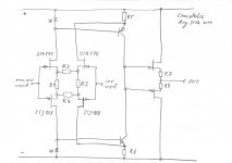
What would you expect from a configuration like this?
The input stage does not need additional components for biasing.
It will offer high input impedance and low noise.
R1 and R2 allow adjustment of bias independently from adjustment
of gain and degeneration which is solved by R3 and R4....
Last but not least you could use such an OP amp for voltage feedback configurations and current feedback applications as well. In current feedback applications one could use the nodes of R1 as current feedback inputs, or center tap R1...
All the rest of the circuit is mostly standard.
That looks really interesting. I almost understand it.
What would you expect from a configuration like this? ...... All the rest of the circuit is mostly standard.
I'm not sure what you are asking from us. As you observe yourself, the circuit is mostly standard (essentially being a complementary folded-cascode + source follower).
Last edited:
I'm not sure what you are asking from us. As you observe yourself, the circuit is mostly standard (essentially being a complementary folded-cascode + source follower).
The input stage is not that much standard.
...hm, and when we combine this input stage with the second and third stage of John's proposal in posting #179 then it starts to look really nice.
Edit:
Nevertheless the basic circuitry of John's posting #169 (I guess source resistors at the output MosFets would be necessary for a real life set up to stabilize and linearize the output stage) is still my favorite, because it has essentially just 6 transistors and you only need matched, what you can get matched. Means it can be optimized without having exactly complementary types. Definitely worth to spend some time with !
Last edited:
Let me offer an example of a simple, elegant, balanced circuit that can be made into the highest quality amplifier, preamplifier, or whatever, with a minimum number of parts.
This is NOT my circuit, and it is at least 40 years old, but Constellation makes world class amps with it, today. I give the credit to Bascom King, but it might go back earlier, I don't know.
John,
For me, the most interesting aspect of this topology is the totem pole output stage design and it's interface to the diff. VAS. Could you make any comments specifically about the output stage to VAS interface and asymmetrical operation?
Scott,
A SMD dual JFET in SOT23 is too good for me to give up, so I went back to the Toshiba website.
It says (see attached) internal connection common source.
So it can at least be used for input LTP.
Toshiba never says whether their FETs can be used with D/S swap.
All the ones I tried can, even though some has a slightly different Idss when reversed.
But this is solvable even if the lower FET has lower Idss when reversed.
Just tie a resistor or a CRD from Vout to the negative rail.
So I am still on for this one.
Patrick
Someone should test a few of the duals. If they isolate the halves (before hardwiring the channels together) the same way they do in the obsoleted parts like the 389, there are no parasitic diodes to conduct other than via reverse leakage (I tested this with the 389, facilitated by their bringing out a lead for the substrate --- which they then tell you to float
 ). I think they just have blinkers on as far as the possible different configurations. But maybe not ---perhaps the hard wired "sources" are part of a structural change to simplify isolation. Testing will tell.
It's interesting that the model published for the BF862 shows markedly different parasitic (i.e., "contact") resistances in series with the designated "drain" and "source". However, when I tested a few there was virtually no difference in on resistance for normal or reversed connections. BTW those parasitic resistances start to become important at high drain currents and limit the already-slow rate of improvement of transconductance and noise reduction.
This is a VERY RATIONAL design.
I bet this was the answer everybody was seeking for...
In addition to Ken's question, I am wondering whether the natural output impedance (without feedback) is low enough to be called a OP amp output stage. To me it appears more like both output MosFets would act like inverse controlled currents sources and consequently would deliver a high output impedance.
...on the other hand, there is no proof that only circuits with a natural low output impedance sound good.
I wish you'd stop calling me Surely.Dumped into a big hopper??? Shirley you jest..
I'da thunk either an expanded wafer, or waffle pack..
jn
No, I was speaking with poetic license (although until Scott posted I had no idea what they really did, but knew that positional adjacency information was either lost or not taken into account).
Appeal to all: can we please reference the design we're speaking of when we post? When other references are interspersed one is left scratching the head as to which is meant.
It doesn't always have to be a quote, but something like "the schematic shown in #231" would remove ambiguity.
It doesn't always have to be a quote, but something like "the schematic shown in #231" would remove ambiguity.
Scott,
A SMD dual JFET in SOT23 is too good for me to give up, so I went back to the Toshiba website.
It says (see attached) internal connection common source.
So it can at least be used for input LTP.
Toshiba never says whether their FETs can be used with D/S swap.
All the ones I tried can, even though some has a slightly different Idss when reversed.
But this is solvable even if the lower FET has lower Idss when reversed.
Just tie a resistor or a CRD from Vout to the negative rail.
So I am still on for this one.
I think Dave posted the wrong link.
Here is the link to John's circuit using N-JFETs as input.
http://www.diyaudio.com/forums/anal...discrete-opamp-open-design-4.html#post3138300
And I also put it here.
I'll do a PCB layout in SMD. I like this.
Patrick
Ugly. Too many FET's.
For the input stage for high Zin (but they will need cascoding) ok, but for the rest of the circuit I would go bipolar. I guess the 8 trannie limit is off the table. 10ppm at 20 kHz 12 V pk into 600 Ohms easily achievable with 11 or 12 active devices, but to get to 500ppb I am compelled to got to 14 or 15 active devices.
Appeal to all: can we please reference the design we're speaking of when we post? When other references are interspersed one is left scratching the head as to which is meant.
It doesn't always have to be a quote, but something like "the schematic shown in #231" would remove ambiguity.
He mentioned BJT version of Blowtorch presented here.
I don't like bipolars, so the first one John posted will do for me. But everyone to his own taste.
Also the small Dual FETs allow a single aided layout on a DIP8 footprint.
So it gets my vote.
The circuit in post#240 I also like, and can be made with all FETs.
But with no more P-FETs widely available, it does not lend itself to the general public who do not have private stocks.
Cheers,
Patrick
Also the small Dual FETs allow a single aided layout on a DIP8 footprint.
So it gets my vote.
The circuit in post#240 I also like, and can be made with all FETs.
But with no more P-FETs widely available, it does not lend itself to the general public who do not have private stocks.
Cheers,
Patrick
Attachments
Well, that was succinct.
The topology used to be almost a Standard one before complimentary push-pull and current-mode fb topologies replaced it.
The reason for that output stage is same as for the diff stages before it - at the time good compliments were virtually non-existant and better match was found with same type transistors.
I used the same topology for my passive RIAA phono stage around 1980-ish but with jfet front end and bipolar Vas for high gain/gnfb and compl bipolar output. Distortion is very low and good PSRR as well could be attained. At that time, the HP thd meter limit was .0018% -- the circuit was better than that and used 6 active transistors (not counting current sources). Today, I think i would use Scott's circuit if i wanted a modern high gain linear circuit.
-RNM
Last edited:
> and three spare PINs for tapping into the circuit for "other" duties/corrections/compensations
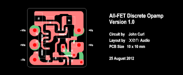
0.4mm plate through holes to connect top layer to bottom layer.
I did not quite manage to get it all in one without jumpers.
And I am sure you don't want to solder 0.4mm enamel wire jumpers.
Patrick
0.4mm plate through holes to connect top layer to bottom layer.
I did not quite manage to get it all in one without jumpers.
And I am sure you don't want to solder 0.4mm enamel wire jumpers.
Patrick
He mentioned BJT version of Blowtorch presented here.
I was talking, among other things, about JC's "rational" design remark, which wasn't clear to me. But in general, we have a tendency to post thinking it is going to appear in immediate succession to what we're referring. And that's often not the case in a busy thread.
Let me clarify things for you all: Over the decades, I have had a series of 'requirements' for making an audio gain stage, developed after years of making prototypes. This designs meets MY criteria, but then I designed the whole thing and put it into a power amplfier, 30 years ago. I guess I should mention that, but that is NOT why I said that it was 'rational'. I meant that this design example meets MY criteria, and does not fall down in some way. Now, if I am allowed, I will try to show where many other designs fall away from meeting the criteria that I find useful and important. Not ALL designs are failures in some way, but they have yet not been presented here to any degree, recently.
Attachments
- Home
- Source & Line
- Analog Line Level
- Discrete Opamp Open Design