Scott -- Yes, it was thru 50K control contacts and all. The pot was about 10+ years old (Alps). No series R issues were found -- tested to 100K source. The C of those jFEts are very low. Used junk resistors. No special attempt to make it best possible - to sqeeze everything out of it. Different goals and appl. However, it too can be tuned up and I would start that, just for the heck of it, if I wasnt leaving for Asia in 2 days. But anyone pls sim away on it. I'll still have Internet some of the time. Not sure about Burma.
Circuit could use a little more OS drive and bias for the super-duper low thd results at 30 Ohms... as you alluded to. And, higher voltage devices and lower Cin output devices for +/-24v appls etc. for PRO use. Then it will be super-tuned.
However, I can't measure below what I got... probably mostly noise from thermal and power supply... though FFT showed the harmonics as such from the analyzer output. PS would also have to be upgraded even further to get that last drop of my blood from it. Something for a sim with perfect PS -who knows what that would produce for THD results. It'll be my first fall project when I return from my adventures abroad or others can play with it now. I do not want to start adding on to it, transistor wise. That is a whole other thing/direction - and probably not needed to get even lower THD (IMNSHO). But you DO have to match devices-select them- to get the lowest levels I get..... a down-side to using simpler symetrical circuits with moderate gnfb. Thx -RNM
Last edited:
I think you need to cascode the jfet input stage. And I think you need to go back to the + and - 30v ideal power supply rails. Ray
At 60v the cascodes become a mess since at that point they have to be either bipolar or something like a 2N7000.
OTOH I just ran it with cascodes and even a 100K pot is OK. We shouldn't go all the way back to one circuit for everything. I think a version with simple FET cascodes (gate tied down to bottom source) would be a good place to leave one (only 4 extra devices). We need to pick a Vds that keeps the input FET's linear.
Looks tight on the J111 .7V typ. but on the good side 5mA is the 0 TC point.
Last edited:
Yes, it was thru 50K control contacts and all. The pot was about 10+ years old (Alps). No series R issues were found -- tested to 100K source. The C of those jFEts are very low. Used junk resistors. No special attempt to make it best possible - to sqeeze everything out of it. Different goals and appl. However, it too can be tuned up and I would start that, just for the heck of it, if I wasnt leaving for asia in 2 days. But anyone pls sim away on it. I'll still have Internet some of the time. Thx -RNM
I forgot you were doing only .25V or so input, the distortion goes as Vin squared.
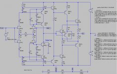
Don't the CCSs, J1 & J2 isolate Q6, 7, 8, 9, 11, 35 and hence Q15 from the signal path?
I can see a signal path through Q15 on some of the later 'symmetrical' versions but not on the simpleeek
Or are there some missing tracks on #1380
ricardo
The intent was to only change the input stage, yes the lines were JPEG'd out.
Hmmm, this should probably be looked at by somebody who understands the subtleties, tried 3 complementary pairs and got DC output levels of 1, 4.5 and -7 volts. My problem, LTspice, or something else ...?
Well, I've spent the last 10 minutes trying to upload a couple of files to attach -- Jeez, I'm sick of braindead software, glad to be out of that game ... try again later ...
Tried again, still not working ...
Hooray, tried a different browser, could be a coincidence, we're cooking ...
Frank
Well, I've spent the last 10 minutes trying to upload a couple of files to attach -- Jeez, I'm sick of braindead software, glad to be out of that game ... try again later ...
Tried again, still not working ...
Hooray, tried a different browser, could be a coincidence, we're cooking ...
Frank
Attachments
Last edited:
I forgot you were doing only .25V or so input, the distortion goes as Vin squared.
What is the affect of a lot of source degeneration on the jFETs re. Vin? Its pretty heavily degenerated. [Design for max 1v input.]
Last edited:
So excuse me if I'm stating the obvious ... but I take it #1397 completely discounts #1380.The intent was to only change the input stage, yes the lines were JPEG'd out.
#1380 was never Guru Wurcer's intention and is just as complex as #1397
#1397's only con wrt to #1380 is the need for Unobtainium FETs
___________________
As far as I can see, there are only 3.5 gain stages; J7-9, Q1&35, Q14&58 and Q56&59. The 0.5 stage is cos the current gain of the last stage is 'sorta' set by R9&10 / R53/44.
It may be the 'alternative' signal path; Q15&16, Q10&13 to Q56&59 has higher gain but my head hurts trying to work this out and would appreciate education from the gurus.
Besides the compensation is in the 'main' path.
___________________
It that is the case, IMHO, it should be possible to equal its performance with a much more conventional circuit ... not too dissimilar from 990. Allowing Iq 8mA, 5mA on the i/p and 25mA total can give a big boost to 20kHz performance of what is a small power amp.
Careful attention to compensation along the lines of Prof Cherry can improve both HF THD and also PSRR.
About the only thing which might be difficult is symmetrical slew rates but this can still approach zillion V/us
___________________
The Unobtainium i/p FETS simplify providing a 'tail' current for the symmetrical cases but is there any other reason for using them apart from Golden Pinnae cred?
___________________
So far, the only practical application mentioned is a headphone amp. On that basis, I think we'd be hard put to equal, let alone better the O2 headphone amp which prompted this article NwAvGuy: Op Amp Measurements
OK. It isn't zillion V/us ...
___________________
Instead of +/- 30V capability, a far more useful requirement would be comfortable 10dBU (6.93Vpp) into 600R on a 9V PP3
For flexible use in EQ & filter circuits, no nasty TL07x or LM4562 latching.
For other stuff, I'm happy with AD797 .. even its high In.
___________________
... in the interest of fun, exchanging ideas and hoping for pearls of wisdom from Guru Wurcer etc.
Its an OPA - have a cigar !
Its a universal design for high end audio applications; Use it for what ever you need it to be; preamps, cross-overs, EQ/filters. Its a discrete OP-Amp. Just like the forum title says. A fine SW-OPA has emerged. I wanna see pcb's when i get back... I'll be all beat up and tired and shot at ('cause I'm American)... so a nice quiet time doing pcb stuffing will be in order.
-Thx RNM
Last edited:
Excellent idea, Scott. Please do.
/S
/S
Rather than answer questions piecemeal how about I put a device by device description in the articles section, this is a holiday weekend I might have some time.
@kgrlee:
oh common! dont put the 'feedback'll'fix everything' amp up as a target. for starters clipping at a standard 2.1v line level input is not something I expect this amp to do.
besides, it would appear destruction/negativity and promotion of an unsustainable business model is what prompted the O2, quite the opposite of this.
Err..rh? Would you like to specify when you expect this (Wurcer) amp to clip if it was configured as a headphone amp like the O2?for starters clipping at a standard 2.1v line level input is not something I expect this amp to do.
This would help us tie down your performance requirements for Guru Wurcer's fine design. Presently the only common thread in all the versions is zillion V/us slew.
You may like to check out why the O2 doesn't have this. We, of course, would welcome your explanation why zillion V/us is necessary.
I think Mr. Wurcer would like to ensure his design at least equals the O2 both objectively & subjectively so its a perfectly valid target for the headphone amp application.
BTW, the O2 isn't a "Feedback fixes everything" design. It's actually quite sparing in its use of this evil sauce. Only enough to meet the performance requirements and everything else must be right too.
Some pointers to an answer - it appears the JFET models I'm using may need to be better quality; I noted that the inter source resistor R5 on dadod's version was 50R rather than 250R, this made a big difference to stabilising the DC output point. But, reducing the value again triggered instability, more to be done ...
Frank
Frank
Last edited:
Some pointers to an answer - it appears the JFET models I'm using may need to be better quality; I noted that the inter source resistor R5 on dadod's version was 50R rather than 250R, this made a big difference to stabilising the DC output point. But, reducing the value again triggered instability, more to be done ...
Frank
It is not my version, 50R is original Wurzer value.
Why do not start with my simulation file, unzip it in separate directory and you'll have all you need, with the models also.
Only difference, I did, is the compensating cap connected to the left side of 50R resistor instead to the ground, and LED instead two diodes for the cascode. After that you can start to change components, output transistors first.
dado
Thanks for that, dadod. I've already looked at your verson, and there's no real difference between the two, apart from the LED and single diodes, not sure what you mean about the comp cap. Yet you were getting close to a null DC output, didn't make sense.
Anyway, in the end it came down to the JFETs subcircuit being very sensitive to the source resistors, if you change a single 25R to a 26R say, then your version shows the same symptoms as mine ...
Frank
Anyway, in the end it came down to the JFETs subcircuit being very sensitive to the source resistors, if you change a single 25R to a 26R say, then your version shows the same symptoms as mine ...
Frank
- Home
- Source & Line
- Analog Line Level
- Discrete Opamp Open Design