The non-IC discrete here should do that and more, if possible -- Key to design for: be very simple -- use the fewest transistors. Low cost, easy to find parts. Drive low Z. No dc servo. wide OL bandwidth. THD and noise < -100db ref 1v. Gain at a range of 4-10X etal. Others can decide what more can be done by their design. -Thx RNM
You said it not me , " it must be able to also do lower Z at low thd than IC opamp/IC buffer combo. Or what's the point -- just use an IC. -RNM " I just pointed out that there are single IC's that do all of the above (and they even look like op-amps).
Yes, an ADSL driver won't make a good phono pre-amp.
I choose not to particpate in your challenge, do you mind?
Last edited:
John,
I think that I have some of your earlier amplifier designs from Parasound that are about that vintage. One has been sitting for quite some time with all the output devices fried. My fault with an unstable crossover that went into oscillation and the amp was running in bridged mode, couldn't turn it off fast enough. Still want to fix that though. Needs all new NPN and PNP devices though.
I think that I have some of your earlier amplifier designs from Parasound that are about that vintage. One has been sitting for quite some time with all the output devices fried. My fault with an unstable crossover that went into oscillation and the amp was running in bridged mode, couldn't turn it off fast enough. Still want to fix that though. Needs all new NPN and PNP devices though.
You said it not me , " it must be able to also do lower Z at low thd than IC opamp/IC buffer combo. Or what's the point -- just use an IC. -RNM " I just pointed out that there are single IC's that do all of the above (and they even look like op-amps).
Yes, an ADSL driver won't make a good phono pre-amp.
Ok - you get one point for that.
It was thought up to do a best effort in a discrete form.
My question or challenge was -can the limitations/conditions I gave be all met and still do as well or better than an IC opamp? Maybe.
No. Of course, I dont mind, Scott. Just keep doing what it is you are doing is fine. -Dick
Last edited:
Breadboarded a slightly modified version of the circuit in #271 - more or less a JC2 with a diamond out: *** unselected *** J113/J175 in the front-end, BC550/560 in the gain/driver stages, MJE243/253 in the output stage. Even with randomly choosen devices, it rocks - THD < 0.001% @ 1kHz, 0dBV into 30 ohm, only low order.
More to follow.
Ciao,
L.
More to follow.
Ciao,
L.
Attachments
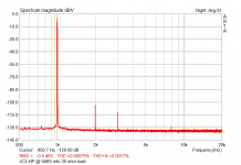
Breadboarded a slightly modified version of the circuit in #271 - more or less a JC2 with a diamond out: *** unselected *** J113/J175 in the front-end, BC550/560 in the gain/driver stages, MJE243/253 in the output stage. Even with randomly choosen devices, it rocks - THD < 0.001% @ 1kHz, 0dBV into 30 ohm, only low order.
More to follow.
Ciao,
L.
Very nice -- esp. unselected and not a sim of ideal perfectly matched parts.
")
Rumbling around back here in the pantry... minimum parts count is certainly something that minimalists will like... and of course anything that has low parts count may also be elegant which is always good.
But equaling the JE990? Is that a valid goal today? I would think exceeding it? No?
Wonder if things like rise time, settling time, overshoot show up in the distortion figures? (I really do not know if there is a direct relationship that can be drawn) If there is not a direct correlation, should these factors be considered as well?
Are all these designs Class B output stages?
Should Class A output stages be under consideration?
At a thermal and power cost, will they yield a better spec (and sounding) op amp?
And, is the claim being made that from a listener's point of view that any device with sufficiently low distortion is audibly not different than the next? Personally, I have yet to find that to be the case. In some instances I have been rather surprised by this.
I'd say the winner is the one that sounds the best, measures the best and not only looks the best on sims and specs... and do we *need a single "winner"?* (rhetorical question)
_-_-bear
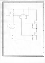
Coluke -- what is the schematic, pls?
I am tinkering with boot-strapping a whole circuit and see if it stays together. Just adds two more transistors. Thx - RNM
Post #271 is a post fm Euvl without any pics or attachments? Post #273 I beleieve contained the first attachment.
Any comments on the other Attachment I seem to have collected somewhere?
Attachments
For the record only, in post #271
http://www.diyaudio.com/forums/anal...discrete-opamp-open-design-6.html#post3140160
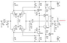
I referred to the schematics published by John in post #168 :
http://www.diyaudio.com/forums/anal...discrete-opamp-open-design-4.html#post3138300
which is attached again here.
Patrick
http://www.diyaudio.com/forums/anal...discrete-opamp-open-design-6.html#post3140160
I referred to the schematics published by John in post #168 :
http://www.diyaudio.com/forums/anal...discrete-opamp-open-design-4.html#post3138300
which is attached again here.
Patrick
Attachments
For the record only, in post #271
http://www.diyaudio.com/forums/anal...discrete-opamp-open-design-6.html#post3140160
I referred to the schematics published by John in post #168 :
We probably need a separate thread for this, aka Kaneda-Constellation-Melcor 1731.
Again, just for the record:
1) Dirt-cheap SOT23 2n7002s simulate fine as the output stage MOSFETs.
2) HF loop-gain can be tamed with gate-to-drain miller caps of 10s of pF on both VAS transistors.
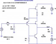
Here's a novel buffer with just 4 actives including a current source. It simulates with THD20 of -95 dB at 2V amplitude into 600R, at a quiescent current of 12 mA.
This topology differs from one published in these forums a few years ago. I hereby exercise my right to name it: Cantilevered-Cascode Buffer. I hereby also exercise my right to place it in the public domain, free of patent encumbrances. No warranty, express or implied, is provided.
This topology differs from one published in these forums a few years ago. I hereby exercise my right to name it: Cantilevered-Cascode Buffer. I hereby also exercise my right to place it in the public domain, free of patent encumbrances. No warranty, express or implied, is provided.
Attachments
Post #273 I beleieve contained the first attachment.
Sorry - you're right: the design is in post #273. I'll post the actual schematics as soon as possible.
L.
> Dirt-cheap SOT23 2n7002s simulate fine as the output stage MOSFETs.
Many devices sim fine as the output devices, including Dual 2N7002 variants in 6-lead SC-70 from both Zetex (Diodes Inc) and Toshiba.
I chose to use Dual devices in SOT23-6 not only because they track each other better thermally, but also they allow a bit more dissipation than the smaller SC-70 packages.
http://www.analog.com/static/imported-files/packages/PKG_PDF/SC70(KS)/KS_6.pdf
Patrick
I like it, a clever form of load current compensation, tuned for the particular load but robust against moderate changes. It is reminiscent of a circuit shown in a short article by Danyuk that I'll try to find a link to, particularly the operation of the one JFET at a low Vds.Here's a novel buffer with just 4 actives including a current source. It simulates with THD20 of -95 dB at 2V amplitude into 600R, at a quiescent current of 12 mA.
This topology differs from one published in these forums a few years ago. I hereby exercise my right to name it: Cantilevered-Cascode Buffer. I hereby also exercise my right to place it in the public domain, free of patent encumbrances. No warranty, express or implied, is provided.
With my particular models for the devices and the load R, I find that fine-tuning R2 (nearest E96 value 2.43k) can drastically reduce 2nd harmonic and as well reduce output offset, leaving 3rd strongly dominant and overall distortion for 2V peak in at 1kHz to about -118dBr. The bandwidth is also very high (around 50MHz) and a bit of peaking is quelled with about 2.2pF to common at the input gate/base.
The optimization of R2 is not frequency-independent or load-independent, but at 20kHz 2V peak the again-dominant 2nd brings things up to about -104dBr.
- Home
- Source & Line
- Analog Line Level
- Discrete Opamp Open Design