Those boards do look pretty manageable. This is the cordwood construction I remember:
This sort of thing reminds of the Carver cube,
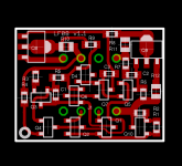
Updated layout to use SOT89 pre-drivers, and improved placement and routing to avoid running traces between resistor pads. Things are now spread out a bit more to simplify assembly.
The practical implication is that the pre-driver bias current can now probably be raised to 10 mA or higher (maybe much more for low-rail applications including headphone amps), which makes it feasible to omit the output stage altogether for various high-Z loads - it essentially becomes a BJT Kaneda-type opamp.
Of course, an external Vbe multiplier and output stage may be used as before (maybe a 3-diode chain between pins 8 & 5 biasing a complementary darlington pair like TIP142/147 for Class-B operation in the simplest case). MOS, Laterals, etc. are all feasible with a Vbe-multiplier.
Attachments
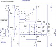
Merry Christmas, folks! Linus has a tradition of giving an X'mas gift of a Linux kernel release in December every year, which I'll try to emulate as well. Here is the simulation schematic of the current version of the LF08 discrete opamp incorporating most of the useful tweaks and mods so far - thanks to XRK971 for the dual-output mod, and Dogearbass for his investigation of a slew-rate issue on square-wave inputs that led to the addition of C2 to mitigate it.
As always, this remains work in progress, and no warranty, express or implied, is provided - use at your own risk.
As always, this remains work in progress, and no warranty, express or implied, is provided - use at your own risk.
Attachments
Merry Christmas, folks! Linus has a tradition of giving an X'mas gift of a Linux kernel release in December every year, which I'll try to emulate as well. Here is the simulation schematic of the current version of the LF08 discrete opamp incorporating most of the useful tweaks and mods so far - thanks to XRK971 for the dual-output mod, and dogearsbass for his investigation of a slew-rate issue on square-wave inputs that led to the addition of C2 to mitigate it.
As always, this remains work in progress, and no warranty, express or implied, is provided - use at your own risk.
Happy Xmas and New Year to you too Linuxguru. Very nice design - do you have Gerber files for the dual output variant? I was quite surprised at the predicted performance when driving 50ohm headphones. Thank you for the holiday gift.

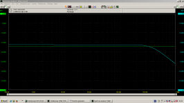
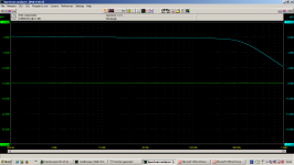
Linuxguru, at first I could not understand how your circuit work, so I have simulated it on LTspice and now I understood DC operating point, but still does not understand the phase compensation scheme.
The LTspice shows the 2nd pole sits 60kHz and transition frequency is 1.5MHz. It is not stable without another compensation except very high closed gain.
The LTspice shows the 2nd pole sits 60kHz and transition frequency is 1.5MHz. It is not stable without another compensation except very high closed gain.
... does not understand the phase compensation scheme.
The LTspice shows the 2nd pole sits 60kHz and transition frequency is 1.5MHz. It is not stable without another compensation except very high closed gain.
C1-R4 and C3-R6 are Miller compensation around the current mirror and VAS respectively. There's also C4 for the cascode Q7 - which can probably be increased up to 47 pF to tame any instability. LTSpice shows it as unity-gain stable with the values shown, but compensation values may be considered to be work in progress. If C4 is too high, it will have an impact on THD20 as well as sonics.
A physical prototype has been built by dogearsbass with C4 omitted and apparently stable at closed-loop gain of 3, i.e. ~10 dB closed-loop. However, that prototype differs from the schematic above in that it uses only single output pair, RC across the LTP collectors and no LTP degeneration. I'd guess intuitively that my version in post #3323 above is more stable than dogearsbass prototype, but YMMV. You can always play around with the values of C1, R4, C3, R6, C4, LTP degeneration and RC across the LTP collectors (as in the original Melcor 1731) in LTSpice.
Sorry I forgot to write that my simulation was closed loop gain x10 and the transition frequency was 1.8MHz. At the time I tried differentiating compensation in the feedback network.
When I changed closed loop gain to x1 to remove the pole at inverting input, it have less
than 0° phase margin at 8MHz transition frequency.
How did you define the phase compensation elements value? My results may be due to my mistake in the simulation or I used generic 2N2222 and 2N2907 model for the transistors that makes abnormally. Can you upload your simulation file?
OK, here's the .asc from my version of LTSpice - ancient Switcher CAD III. I used stock models of all devices downloaded from NXP long ago, but you should be fine with some generic small-signal NPN/PNPs. The compensation schema as well as values were mainly obtained by old-fashioned trial and error.
(I had tinkered with C4 after I posted the simulation schematic. C4=33pF seems to reduce the peaking on the unity gain AC response. Another alternative is to put C4 on C-B of Q8, in which case it can increased as high as 100 pF without impacting the Gain-BW, though H2 increases a bit - which may actually be beneficial for audible sonics.)
(I had tinkered with C4 after I posted the simulation schematic. C4=33pF seems to reduce the peaking on the unity gain AC response. Another alternative is to put C4 on C-B of Q8, in which case it can increased as high as 100 pF without impacting the Gain-BW, though H2 increases a bit - which may actually be beneficial for audible sonics.)
Attachments
Last edited:
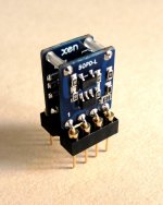
On a couple of occasions in the past, we attempted to build discrete opamps on a DIP8 footprint.
Pass Discrete Opamp in DIP-8 Package
https://www.diyaudio.com/forums/analog-line-level/218373-discrete-opamp-design-28.html#post3184856 __ (post #1379)
They work to a certain extent, but DC stability is difficult to control.
And they are also not unity gain stable, or only marginally.
This is our latest attempt.
This time it is DC stable to +/-1mV at the output with a gain of 10.
Output DC was 3mV after trimming, so 0.3mV referred to input.
It is also unity gain stable. And meets all design criteria.
The basic topology is similar to the JC2 phono module, with all SMD parts.
Is small enough to fit directly on SOIC8 pins.
PCB is 10mm x 13mm x 0.8mm.
Quite happy with the results this time.")
Patrick
.
Pass Discrete Opamp in DIP-8 Package
https://www.diyaudio.com/forums/analog-line-level/218373-discrete-opamp-design-28.html#post3184856 __ (post #1379)
They work to a certain extent, but DC stability is difficult to control.
And they are also not unity gain stable, or only marginally.
This is our latest attempt.
This time it is DC stable to +/-1mV at the output with a gain of 10.
Output DC was 3mV after trimming, so 0.3mV referred to input.
It is also unity gain stable. And meets all design criteria.
The basic topology is similar to the JC2 phono module, with all SMD parts.
Is small enough to fit directly on SOIC8 pins.
PCB is 10mm x 13mm x 0.8mm.
Quite happy with the results this time.
Patrick
.
Attachments
And here is Dual version on DIP8, using a different, single-ended circuitry.
Similar to Fig. 14 of the Pass article :
https://www.passdiy.com/pdf/diyopamp.pdf
Patrick
.
Similar to Fig. 14 of the Pass article :
https://www.passdiy.com/pdf/diyopamp.pdf
Patrick
.
Attachments
[...]Similar to Fig. 14[...]
That leaves quite some room for interpretation...
All FET or all BJT, or..?
Good that you found a suitable p-channel for output.... The basic topology is similar to the JC2 phono module, with all SMD parts....
Discrete OpAmp on BF998-BSS84
My 5 cents:
Discrete OpAmp on N+P channel RF MOSFETs: BF998+BSS84.
Software model only. Made with MicroCap 9.0.
Spec:
Open loop gain ~ 60dB.
Bandwidth limit at Gain=1~ 30MHz.
THD at gain=60dB ~0.09% at 8V output.
THD at gain=40 dB ~0.0003% at 1V output.
Schematic:
Currents:
Freq-Phase:
THD-IHD at gain=60dB:
THD-IHD at gain=40dB:
Voltages:
Circuit: View attachment Discrete-OpAmp=BF998-BSS84=Diff=Classic-CM.zip
R3, R4, C2 - just placeholders to debug the schematic.
Last edited:
- Home
- Source & Line
- Analog Line Level
- Discrete Opamp Open Design