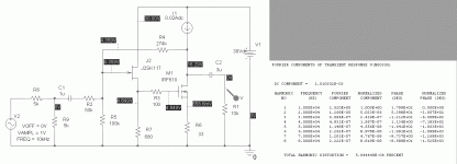
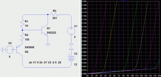
A week or so ago, I decided to do a simulation of a lineamp circuit using a mosfet with drain-to-gate feedback, a configuration that can look like an extremely linear triode. I wanted to try something triode-ish that could be done with readily available parts rather than busting my a** trying to score some SITs. I was shooting for a gain of ~5 or so, and the values used in the simulation shown below get me there. I was expecting THD in the tenths of a percent or so, and was shocked at the simulation results.
Attached is the circuit I simulated and the simulation results. The jfet buffers the mosfet gate, allowing a high impedance feedback network and also providing some heft to bull past Miller capacitance. Using my trusty favorite the PN4393 or the 2SK117 for input duty nets me similar results, with a little bit of tweaking necessary to center the output mosfet drain voltage.
In retrospect, the setup looks very much like the guts of my "Half Nelson" Class A amp, described in the Pass Amps forum. In real life, I plan to use a depletion mode mosfet current source of some sort to replace the perfect current source at the mosfet drain. The pair of resistors at the input was used to see how the distortion would fare when the circuit is driven with something besides a perfect voltage source. I'll use a 10k volume pot in front of the real deal. I'm pretty sure someone has already done a circuit very similar - it's too simple. I really don't care if I happen to be re-inventing the wheel. Am I gonna build this? Heck, yeah! My only quibble is that the circuit is inverting, and I like a non-inverting line amp.
I'll probably replace the IRF610 of the simulation with a smaller mosfet like the MPF960, a nice little fet in a TO-92L package (sadly discontinued, but I still have some). The TO-92L will handle 1/2W or so of dissipation with no problem.
Attachments
I share your surprise at the THD figure the sim is predicting. Makes me wonder if there is some complementary distortion cancellation taking place between the JFET and MOSFET. Nice little circuit. With sufficient bias current it would probably make for a good headphone amp as well.
Last edited:
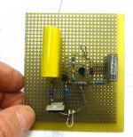
I'm using an MPF960 in the prototype, as it has about 1/2 the input capacitance of the IRF610, and it's in a TO-92L package that will dissipate the 300mW or so required by this application. The TO-220 device you see on the breadboard is a Supertex DN2540N5 depletion mode fet, used as the current source load for the output mosfet. If I get within a factor of ten of the THD shown in the simulation, I'll be one happy camper.
Last edited:
The SIT simulation thing seems to have originated with Schade, who was
simulating triodes with pentodes using this sort of feedback. With your
input Jfet, the input impedance is high enough to be usable.
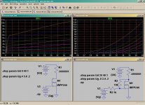
Here is a graphic that one of our members posted (can't remember who,
sorry).

simulating triodes with pentodes using this sort of feedback. With your
input Jfet, the input impedance is high enough to be usable.
Here is a graphic that one of our members posted (can't remember who,
sorry).
Attachments
With your
input Jfet, the input impedance is high enough to be usable.
sorry).
Is this one of the keys to this circuit?
It was certainly what I had in mind when I used a similar circuit for the "Half-Nelson" amp, (something I ginned up in 2007 before I found out about all this Schade stuff) and here as well. The jfet allows a high impedance feedback network and a respectable frequency response, due to the low jfet capacitance and the source follower drive to the mosfet gate. I'm going to use my results here to do another spin on the Half Nelson, possibly using one of the Ixys depletion mode fets on top of the output mosfet. I'll post circuit and results for that back in the Half Nelson thread when I get around to it.
Yep, I saw the simulation (or something similar) shown in post 8 in one of the tube threads. The "Schade Fet" has cropped up several times, once as a ringer in a "name that tube curve" threrad.
Yep, I saw the simulation (or something similar) shown in post 8 in one of the tube threads. The "Schade Fet" has cropped up several times, once as a ringer in a "name that tube curve" threrad.
Last edited:
I think one other additional key to the design is to bias the fet fairly hot for high transconductance. This, coupled with the current source loading, gives one a lot of gain to feed back. Using the IRF610 with a good heat sink, one could really go for the gusto and use 50-100ma of bias current for even more transconductance. With a little higher gain, you'd get that headphone amp that Mr. Newton was talking about...
No Schaded single curveset accurately mimics a triode.
The way real triode curves "lean to the right" is probably
aggregate of many parallel triode paths of differing cutoff.
I think was Smoking who proposed this?
Anyways, I tested that theory by throwing many different
Schaded curvesets into a blender. I found that it seems to
require bare minimum of four curvesets to make a triode
curveset that leans in believable fashion.
Faking a SIT might be one curve only, I don't know...
I've always said "triode-ish", unlike the unmodified device, which is "pentode-ish".
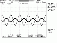
Anyway, the composite device stands on its own. I'll find out how good it actually is when I hook it up to my distortion analyzer. It could be 100X worse than the simulation in real life and still be pretty damn good, considering the parts count.
Anyway, the composite device stands on its own. I'll find out how good it actually is when I hook it up to my distortion analyzer. It could be 100X worse than the simulation in real life and still be pretty damn good, considering the parts count.
Current works as well as voltage.
What I mean is: I didn't need a base
resistor to convert voltage to current.
The divider is also the base resistor.
It doesn't matter the voltage is wrong
due to the base current, only matters
the base current is right. And it is...
High impedance gate unnecessary.
The leakage current causes no error.
Attachments
Last edited:
I've done some messing about in simulation with the bipolar version shown a couple of posts ago with results so far that are unimpressive compared to the original Jfet/mosfet circuit posed at the beginning of this thread. That one appears to satisfy all my requirements for a relatively low gain line amp except for being inverting. I may have time to make some distortion measurements on my breadboard this weekend, if I can find the BNC cables I just bought a week and a half ago...
Nice work, thanks for posting.
I'd like to see what happens if you went for less gain, say 2-3? I assume you do that by increasing degeneration/the bottom resistor on the Mosfet. Also, any idea what output impedance is as shown?
What about the BS170? They are cheap but should handle 20ma, 830mW total. I have a bunch here for something else.
- Status
- This old topic is closed. If you want to reopen this topic, contact a moderator using the "Report Post" button.
- Home
- Source & Line
- Analog Line Level
- If You Don't Have a SIT, Fake It...