Hi,
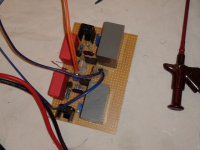
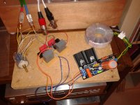
I put on a breadboard your first schematic as you can see on the pictures, to try it, as I need a pre with a little bit of gain.
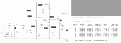
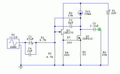
I made it as per the attached schematic, with the following changes: R2 = 47K, R4=180K // 5pico silver mica (I also had some overshoot on my 10khz square, but now looks fine as you can see, also wanted to reduce gain a bit so I used an 180k), for R7 I used a trimmer in order bias the circuit (in my case around 510ohm), and for current source I used an IXYS IXTP01N100D set at 35mA.
For voltage regulation, a Salas BIB set at 30V and 210mA.
I used a 10k pot at the input.
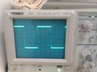
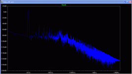
Measurements on the scope were fine, with a bandwidth of 330kHz.
However, when I listen to it I got a quite high level of noise for my liking. Keep in mind that I use horn speakers which are more than 100dB sensitive. On less efficient speakers, this maybe tolerable, but not in my case.
Gain was still high for needs. As I understand, gain is determined by the ratio of R4/R2. Is it possible to reduce their values, without having to add a bigger cap at the input?
Despite that, I quite liked the sound initially, especially the bass was very good.
Any help on all these will be appreciated.
I put on a breadboard your first schematic as you can see on the pictures, to try it, as I need a pre with a little bit of gain.
I made it as per the attached schematic, with the following changes: R2 = 47K, R4=180K // 5pico silver mica (I also had some overshoot on my 10khz square, but now looks fine as you can see, also wanted to reduce gain a bit so I used an 180k), for R7 I used a trimmer in order bias the circuit (in my case around 510ohm), and for current source I used an IXYS IXTP01N100D set at 35mA.
For voltage regulation, a Salas BIB set at 30V and 210mA.
I used a 10k pot at the input.
Measurements on the scope were fine, with a bandwidth of 330kHz.
However, when I listen to it I got a quite high level of noise for my liking. Keep in mind that I use horn speakers which are more than 100dB sensitive. On less efficient speakers, this maybe tolerable, but not in my case.
Gain was still high for needs. As I understand, gain is determined by the ratio of R4/R2. Is it possible to reduce their values, without having to add a bigger cap at the input?
Despite that, I quite liked the sound initially, especially the bass was very good.
Any help on all these will be appreciated.
Attachments
If you used a pot to set the bias level and kept in in, this might account for the noise you mention. Even a nice Noble 50k volume pot will hiss like a nest of snakes with some DC across it (I know from sad experience). If the pot is still in place, try replacing it with a fixed resistor equal to the pot resistance at its current setting (just use a meter to measure) and you may be very pleasantly surprised. Since this is, after all, a line-level amplifier with low gain, I can't think of anything else that could account for audible levels of noise, even with sensitive speakers.
BTW, kudos to you for actually taking the initiative to build this circuit and listen to it. You actually beat me to listening tests. I'm still playing around with my distortion test setup so I can get realistic and consistent readings.
BTW, kudos to you for actually taking the initiative to build this circuit and listen to it. You actually beat me to listening tests. I'm still playing around with my distortion test setup so I can get realistic and consistent readings.
Salas, the whole point of this exercise was to be able to push up the impedance of the feedback network and yet have some drive available for the mosfet gate. The way you show it, you really need that electrolytic (or a great honkin' film cap), plus a buffer to drive the buffer.
One variation I'm thinking of trying is to replace the bottom resistor of the output voltage centering/gain network (R5, per the schematic in Post 41) with an active current sink. A low IDSS, low leakage electrometer fet like the PN4117 would be just the ticket as an active current sink for the few 10s of microamps that are needed to properly set the bias. Just a thought...
I'm currently working on a board that incorporates all the cascode enhancements shown in previous posts, plus an onboard shunt regulator. I'm curious to see how it will perform in my distortion test setup.It would be interesting as well to have it drive a simple buffer and a pair of headphones for a subjective evaluation. I may adopt this approach so I can avoid ripping up my living room setup every time I have a bright idea...
I'm currently working on a board that incorporates all the cascode enhancements shown in previous posts, plus an onboard shunt regulator. I'm curious to see how it will perform in my distortion test setup.It would be interesting as well to have it drive a simple buffer and a pair of headphones for a subjective evaluation. I may adopt this approach so I can avoid ripping up my living room setup every time I have a bright idea...
Salas, the whole point of this exercise was to be able to push up the impedance of the feedback network and yet have some drive available for the mosfet gate. The way you show it, you really need that electrolytic (or a great honkin' film cap), plus a buffer to drive the buffer.
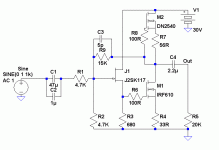
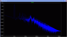
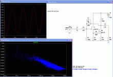
Was just an idea to check where the hiss comes from on those horns. Valid points the drive difficulty and the large input capacitor indeed. So I went on investigating the theoretical THD differences. I run two FFT on LT SPICE. First is for the ~5x gain high impedance feedback network, the second is for the low impedance ~3x gain. Both on 20mA depletion mode Mosfet CCS setting. Simulated SNR -91dB HiImp, -104dB LoImp.
Attachments
That's very nice, but if you screw up the signal source trying to drive the low impedance, you're not exactly ahead of the game. You might try increasing the bias current in the mosfet. That definitely worked for me in terms of reducing the distortion. I'm biasing the input jfet at ~5 ma, which should work nice for the 2SK117.
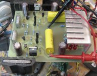
Here's the latest effort - a bit neater that my first. There's two channels and an onboard shunt regulator. The output mosfet and its current source drain load are both cascoded. One channel exhibited high amplitude oscillations at ~350 kHZ (so low?), while the other looked stable. About 3" of "gimmick" capacitor was applied to the feedback resistor of both channels. It stopped the oscillation on the one channel, and did not obviously destabilize the other. Next up are tests to determine what is going on. I'll post schematics when I'm reasonably satisfied.
Attachments
Hi Wrench,
here is my take on "turning a (MOS)FET into a SIT/triode". Fair Zin, low Zout, BW(-3dB)=1MHz, rail-to-rail swing (almost), high PSRR, Id about 15mA, sounds wonderfull - what more could a man want ?
Built, tested, measured (except for THD) - here is the schematics:
here is my take on "turning a (MOS)FET into a SIT/triode". Fair Zin, low Zout, BW(-3dB)=1MHz, rail-to-rail swing (almost), high PSRR, Id about 15mA, sounds wonderfull - what more could a man want ?
Built, tested, measured (except for THD) - here is the schematics:
Attachments
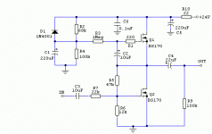
Yes, it's called a gyrator (fake choke - the most appropriate load for the fake triodeR2-4, D1, and C1 are biasing network for top fet?
). Voltage divider R2/R4 sets the gate of Q1 at about 2.5V above Vcc/2Right. It sets the gain and ZinR5/R7(schade component)
No. Voltage divider R5/R6 sets the Id. R5 is already involved in gain setting so the R6 is the one to be manipulated to set the Id (I find the 15mA to be an optimum value)and R6/R7?
As always, Juma, a clear and easy to understand explanation. I don't know why less thinking R5/R6 was feedback, didn't click that these were enhancement mode devices and needed a positive voltage at the gate. I think I have seen the gyrator, minus the diode and with cap going from divider to ground, used to bias the top Jfet in an SRPP type circuit. I have been watching this thread as I am considering trying to use LU Jfet in FE for BA output stage and wrenchone always interesting circuits if for no other reason than just learning. Thanks to both of you.
Nice board wrenchone.
Waiting your final schematic.
I did try salas suggestion with lower resistors. Noise was down but distortion was higher.
With less sensitive speakers maybe there is no problem.
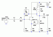
Hi Vgeorge. Having a suspicion also about the CCS amplifying its degeneration resistor's noise enough for your high sens horn speakers, I looked in to just a resistor current source. So I brought back your input impedance higher for your source and pot to better handle, hoping that if there was hiss contribution by the CCS maybe we can trade what we last time cut by lowering Rf/Ri. If you still got it handy its an easy mod to test. Sims >30mA for M1 and a bit more THD 2ndH in the mix. R7 should be a 2W part.
Attachments
- Status
- This old topic is closed. If you want to reopen this topic, contact a moderator using the "Report Post" button.
- Home
- Source & Line
- Analog Line Level
- If You Don't Have a SIT, Fake It...