Well, not to throw stones, but the Pass B1 buffer isn't exactly complex and elegant.
I suppose I can delete the C4 capacitor. Offhand I'd say it shunts HF to -32V rail, but what do I know. It's 5pF from what I can gather by looking at the board.
I think this is a mistake. Conside the rails as short to ground at AC (because the power supply impedance is usually considered low to ground, and you nornmally have decoupling caps).
I could understand this if the cap was connected between the output and inverting input (although there would probably be some stability issues . . . )
OK, I can leave it in, no big deal.
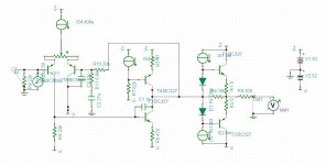
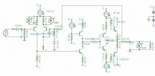
I designed a push pull output stage for it.
I built this in Tina, a SPICE program, using different transistors because they didn't have models for the original ones. I added a simple push pull output stage. Distortion is 0.0016% @ 350mV and 1kHz input. Gain is about 5. I think it's pretty good considering I'm a newbie at this.
Attachments
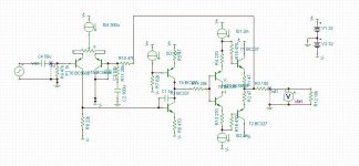
I worked on this some more and came up with this. I had neglected to place a load on the previous design, and the input voltage generator was in the wrong place, as well as other things not optimum. I decided to use a diamond buffer output stage also. With 200mV in, 10kHz and 10kohm load, distortion is 0.0025%. At 500mV it's about the same. At lower frequencies, the distortion is about half (0.00107%). Of course, this is an idealized, simulated circuit, but it's still fun to fool around with it.
I've twiddled with just about every resistor and capacitor in this circuit, as well as adding and removing components. I figured out that the class A voltage gain stage is extremely sensitive to load and the constant current arrangement is extremely sensitive to the voltage divider bias network. I had to add the 28kohm resistor between this stage and the diamond buffer to reduce the load on the voltage gain stage. I guess the input impedance for the diamond buffer isn't that high. Anyway, I'm open to comments and suggestions on this circuit.
Even with 2volts input, distortion is still only 0.004%. dang.
Attachments
Last edited:
I think this is a mistake. Conside the rails as short to ground at AC (because the power supply impedance is usually considered low to ground, and you nornmally have decoupling caps).
I could understand this if the cap was connected between the output and inverting input (although there would probably be some stability issues . . . )
It turned out that this little capacitor reduces distortion, so it's in. I've played with the value and I think it's dependent on the kind of transistor used for Q2. With the BC 560 I got 15pF as ideal, lowest distortion at 10kHz.
The distotion levels you are getting are high given the signal levels and the type of circuit. Any good the little cap is doing is masked by other serious problems.
The good news, is the cures are easy to implement.
Your LTP tail current is set to 300uA and the LTP load resistor is 22k. This is far too high and means that the LTP is grossly unbalanced, leading to distortion (mainly 3rd). Remove R6 (470 Ohm resistor) - you dont need it in a small signal amplifíer like this. To balance the LTP collector currents, R8 will be in the range of 3800 - 4200 Ohms. To do this, measure the LTP collector currents, and adjust R8 until they are within 0.5% of each other - the closer the balance, the better.
The base resitors in your diamond buffer are on the high side. In a diamond buffer, you can often get away without these, but if needed (base stoppers to prevent HF parasitic oscillation) then 10 ohms is normally enough.
Similarly, the driver standoff resistors (R4 and R13) are also too high. In most designs you can do away with these, but if needed to set up the correct output stage current, they will tend to be 10's of ohms and not 270.
The output stage emmitter degen resistors are shown at 47 Ohms - this is very high, and necessitated by the high value of R4 and R13. Typically these would be 3.3 to about 5.6 Ohms. To optimze the diamond buffer output stage, set R1 and R2 to 3.3 Ohms, remove the base stoppers, remove the stand off resistors. Run a sim and check the output stage current. If you want class A operation for typical 600 Ohm loads, I'd set the output stage current at 30-50mA (note: much higher than an IC design - but thats one advantage of going discrete!). If its much higher, increase R1 and R2 value - if much lower use the standoff resistors in the driver emitters - you may need 10-30 Ohms at most. Another option here is to tweak the driver current sources.
Your diamond buffer driver current sources are shown at 2mA - this is ok. In a well optimized design using this topology, you can replace the current sources with resistors (10k on 15V supplies works well) and still get outstanding distortion performance.
With these adjustments, you should be able to get distortion down to 30ppm at 20KHz at 10V into a 1k load, and about a quarter of this at 2-3V into 1K.
How to get distortion to below 1ppm (2-3 Volts into 600 Ohm load):-
1. Use a current mirror load in the LTP
2. Add a beta enhancer transistor between the LTP current mirror and the VAS amplifer
One final point:- between the diamond buffer output and your load (after the feedback take off pount), you need to insert a 22 to 50 Ohm resistor to isolate the amplifer fro capacitive loads. without it, you will likely run into stability problems.
Last edited:
Yes, that would make a much better current source. Any small PNP transistor will be fine. There's an easier way to improve that current source, though: just replace R7 with a constant voltage reference like a zener or LED. That will be easier to fit on the existing PCB.I figured out that I can probably replace R7 with a transistor, connecting the base to junction of the emitter of Q3 and R10.
An even bigger improvement is to replace R4 with some sort of constant current source. I see you did that in your later Tina circuit - good!.
No, that's the opposite of what you want to do - it will make PSRR terrible. To get the effect you want, you need to leave R7 as is and replace R8 with a constant current diode. Oops - got that one wrong in the Tina circuit.I figured out that the voltage divider R7 (910) and R8 (62k) draw 1mA, so I can replace R7 with a 1mA constant current diode to improve PSRR.
See comments above. Also; C4 in the original circuit (C3 in the Tina circuit) looks to me like a really bad idea. I can't see that it can be doing anything useful, but it will make stability and high frequency PSRR worse.I built this in Tina...
Good luck!
Wow, thanks everyone for the feedback! I've tried some of the ideas already but none have reduced distortion yet. I tried reducing the LTP load resistor from 22k to 10k but it made the circuit impossible to balance. I'd have to make changes somewhere else to make that work. Removing the 470 ohm resistor in the voltage gain stage made the distortion much worse also. Thanks for the great ideas!
C3 in the Tina circuit has a noticeable effect on distortion. The value is critical.
Swapping the current source and resistor in the bias network for T4 made the distortion worse as well (0.0033% vs 0.0011%). The alternate arrangement was 910 ohms on top with 1ma below.
The input generator setting is 1kHz @ 500mV for all of these tests so far.
Swapping the current source and resistor in the bias network for T4 made the distortion worse as well (0.0033% vs 0.0011%). The alternate arrangement was 910 ohms on top with 1ma below.
The input generator setting is 1kHz @ 500mV for all of these tests so far.
Note, if you are using small signal devices for the output stage (TO-92) you will have to keep the output stage class A current to 15-20mA
They were at 10mA, but now are about 14mA. Thanks!
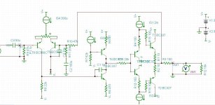
This arrangement gives 0.0009% distortion. I had made an error in the diamond buffer. One of the transistors was a mismatch. I reduced the resistor values in the buffer also. I changed the input transistors to the high hfe version BC550C. I tried the BC550 (and it's complement) in the VAS stage but that didn't help. I tried lowering the differential load resistor from 22k to 4k, and also at the same time eliminated the 470 ohm resistor R6, but that made the distortion worse even after adjusting the trim pot for good DC balance. So, I put it all back and the distortion went way down. The rails on this thing are +/-32volts.
The constant current device in the VAS is set to 5.9mA. The output transistors T1 and T2 are running at almost 15mA.
Thanks again for all the help. I'm trying to get an intuitive feel for this circuit and this TINA software really helps.
For the differential input stage, I measured 159uA flowing through the 22k resistor, so I set the CCD in the tail to twice that value, or about 300uA. That was my reasoning anyway. I tried changing the value for it but doing that just made everything worse. I thought 159uA was a little low... The base of the input transistor sits at around 48mV and seems to be a function of the input resistor. I guess that makes sense since this is a self biased arrangement for the differential pair. The original schematic had the input resistor R9 at 100kohms. I have it at 47k. I suppose I can try changing it back.
I can't easily add a current mirror or any other transistors to this circuit since at that point I might as well perfboard the entire thing.
Attachments
Last edited:
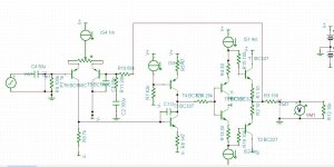
I've got it down to 0.0008% now (1kHz, 500mV in). I made some adjustments in the buffer stage by increasing the current through the first pair of transistors to 4mA, from 2. I changed the input differential also. I thought 300uA was a little low, so I bumped it up to 1mA and changed the load resistor to 7k. This required that I also change the degeneration resistor in the VAS down to 147 ohms. Current in that stage remains the same at 6mA. I also changed the base resistors on the differential amplifier up to 100kohms and the feedback resistor to 68kohms. This increased the bias on the differential pair. T6 is at 65mV and it's partner is at 103mV. I also twiddled with the capacitors C1 and C3. I was working to get the distortion down at 10kHz also, which is now much better.
Thanks again for all the ideas! my head is exploding...
Thanks again for all the ideas! my head is exploding...
Whoops, forgot the figure.
Just to note, the original schematic had the input differential pair running at about 159uA each, that's where I got all this from in the first place. The original input transistor pair is the 2SA1015, which is obsolete.
Just to note, the original schematic had the input differential pair running at about 159uA each, that's where I got all this from in the first place. The original input transistor pair is the 2SA1015, which is obsolete.
Attachments
Last edited:
there is something odd that you have with R8.
What is the LTP tail current?
1.) Half that tail current should pass through R8 and feed the base of the VAS.
This ensures that the emitter currents of the LTP are identical.
Now look at your VAS. What is the base current?
What voltage is required across R8 to make statement 1.) true?
get rid of the VR between the emitters of the LTP.
replace with two accurately selected 10r or 33r or 100r as appropriate for the gain margins that you require.
Last edited:
there is something odd that you have with R8.
What is the LTP tail current?
1.) Half that tail current should pass through R8 and feed the base of the VAS.
This ensures that the emitter currents of the LTP are identical.
Now look at your VAS. What is the base current?
What voltage is required across R8 to make statement 1.) true?
get rid of the VR between the emitters of the LTP.
replace with two accurately selected 10r or 33r or 100r as appropriate for the gain margins that you require.
OK, I replaced the VR with two 100ohm resistors, and chose R8 to make the emitter currents as close to equal as I could. I put volt meters across each of the 100 ohm resistors and adjusted R8 until the meters read virtually equal. I also got rid of the Miller integrating capacitor, since it was adding distortion. I also adjusted the connecting resistor between the VAS and the buffer to 4.7k, which gives minimum distortion. Every change I make I check with the Fourier analyzer. Some things make distortion worse, like adding a bypass cap around R6, and the Miller capacitor as I mentioned. I dunno, these are conventional things normally found in amps, so I'm surprised.
Given the easy conditions of 1kHz input @ 500mV into a 10K load, distortion is now 0.00025%. Distortion was about the same for a 1kohm load.
Thanks for your help!
Attachments
Last edited:
I guess this is kind of a strange problem because there are limitations on what can be done with this circuit without just abandoning the circuit boards I already bought. I already have to perfboard the diamond buffer, which is not hard at all, but I'd like to salvage as much of the existing boards as I can. So, I'm working within the confines of the existing board when I'm dealing with the differential amp and the VAS. Adding a current mirror isn't practical, for example, because I'd have to cut traces on the board, and add stuff and make a mess basically. I can't add another transistor between the two stages either. I can play with the values, replace resistors with CCD's, replace transistors, remove parts, etc.
thanks again for the generous help!
Distortion at 2.12Vrms, 1kHz input is still good @ 0.0017%, into a 1kohm load. Output is 8.45Vrms at that point.
One thing I learned is that "everything affects everything" in this circuit, except maybe the buffer stage not so much.
thanks again for the generous help!
Distortion at 2.12Vrms, 1kHz input is still good @ 0.0017%, into a 1kohm load. Output is 8.45Vrms at that point.
One thing I learned is that "everything affects everything" in this circuit, except maybe the buffer stage not so much.
Last edited:
- Status
- This old topic is closed. If you want to reopen this topic, contact a moderator using the "Report Post" button.
- Home
- Source & Line
- Analog Line Level
- discrete op amp