hello,
i'm building an active line splitter based on BJT transistor
i need to split the line output signal of my tascam us122.
( specs of the card:
Nominal output level : –10 dB
Maximum output levels : +6 dBV )
i will use this splitter to send signal to
* speaker amp 1
* speaker amp 2
* headphone amp
for my audio recording studio
- question 1 -
how can i transform the output db/dbV value to voltage?
i've already build a line splitter, based upon
* AMZ - Guitar Effects & JFET Splitter
* Basic Buffers
schematics attached (VCC is +9v)
i've checked this with a scope and a sine signal sweep (0.3V - from 10Hz to 25Kz), it seams to me that the FFT is 1:1 to the original sine signal.
- question 2 -
is this FFT check right?, i mean, is it right to check the frequency response by looking at the generate FFT during a sine sweep?
- question 3 -
i've also check that the output sine is the same amplitude that the input one, for the sweep, and it seams so. is it a good test?
- question 4 -
there are errors in my schematics?
- question 5 -
there is any opamp good schematics for this?
thank you...
Attachments
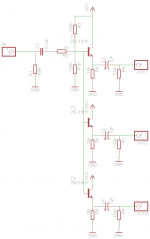
Your circuit is fine although unusual.
R1 could be usefully lower in value.
C1 could be larger depending on the LF response you want.
C2,3 and 4 could likewise be a little larger if you want extended LF response.
Thats all a matter of personal choice.
Using 3 followers is unusual. Remember the bias network has to supply 3 lots of Ib so you want high gain transistors to minimise loading.
It's all very workable but unusual.
Do you need 3 followers ? One opamp output would easily drive 3 outputs, or you could use a quad opamp and use one as a buffer and have the other three as followers.
Even a soundcard output should drive 3 inputs OK.
If you only have a single rail supply avalable the transistor option is absolutely fine.
Even 1 follower would drive 3 inputs.
You could also replace the emitter load resistors with constant current sources.
A follower like this will be good up to many hundreds of Khz when loaded lightly.
Sine wave test is fine, it will also be essentially perfect on squarewave testing too.
For db's and db/v you will have to do some reading and maths...
this covers what you are asking but you need to know impedances and levels,
Decibel - Wikipedia, the free encyclopedia
Your circuit is fine although unusual.
R1 could be usefully lower in value.
C1 could be larger depending on the LF response you want.
C2,3 and 4 could likewise be a little larger if you want extended LF response.
Thats all a matter of personal choice.
Using 3 followers is unusual. Remember the bias network has to supply 3 lots of Ib so you want high gain transistors to minimise loading.
It's all very workable but unusual.
Do you need 3 followers ? One opamp output would easily drive 3 outputs, or you could use a quad opamp and use one as a buffer and have the other three as followers.
Even a soundcard output should drive 3 inputs OK.
If you only have a single rail supply avalable the transistor option is absolutely fine.
Even 1 follower would drive 3 inputs.
You could also replace the emitter load resistors with constant current sources.
A follower like this will be good up to many hundreds of Khz when loaded lightly.
Sine wave test is fine, it will also be essentially perfect on squarewave testing too.
For db's and db/v you will have to do some reading and maths...
this covers what you are asking but you need to know impedances and levels,
Decibel - Wikipedia, the free encyclopedia
thanks,
R1 => 1M, ok?
C1,2,3,4 => i would like an almost perfect freq response, even on LF, from 50Hz to 25Khz, better C1 => 0.3uF - C2,3,4 => 10uF?
dbu, tks i've found the solution with some math.
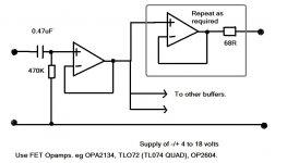
i can use dual supply, or make a virtual ground circuit, so i can also use an opamp for this project. do you know any good schematics?
If you want an opamp it's text book stuff. You must use "unity gain stable" opamps such as OPA2134 (which are duals so you need two IC's). FET opamps also produce zero DC offset.
If you're stuck I can draw a simple schematic later but it's all text book stuff. All stages are connected as followers with the three (if that's what you really want) separate driver stages all fed directly from the first stage. Good practice to isolate each final output via a small resistor of say 68 ohms to ensure total stability with long or capacitive leads.
If you're stuck I can draw a simple schematic later but it's all text book stuff. All stages are connected as followers with the three (if that's what you really want) separate driver stages all fed directly from the first stage. Good practice to isolate each final output via a small resistor of say 68 ohms to ensure total stability with long or capacitive leads.
this is interesting:
How Do I Make a Distribution Amplifier?
expecially this link:
HeadWize - Project: Designing an Opamp Headphone Amplifier (A HeadWize Design Series Paper)
maybe i can use this as a buffer opamp.. ?
How Do I Make a Distribution Amplifier?
expecially this link:
HeadWize - Project: Designing an Opamp Headphone Amplifier (A HeadWize Design Series Paper)
maybe i can use this as a buffer opamp.. ?
Hi,
Why use circuitry at all ? -10dB is 300mV - typical home audio line level.
Most line outputs can drive multiple line inputs with no difficulty.
rgds, sreten.
1) to learn something new - for me, cause i'm a software eng. -
")
2) to split the source output signal without losing power 1:1~ signal
1) to learn something new - for me, cause i'm a software eng. -
I can understand that.
Try something like this. Also with the addition of two resistors in the feedback network the gain of any buffer can be increased.
Haven't shown supply decoupling but it's good practice to add a small electroylitic across the opamp supply pins.
The TL072 is a good choice for a first project as it's stable and draws little current. Very good performance too.
Attachments
Both good points, but regards to 2) what is the output impedance of the thing you're going to plug into this? What are the input impedances of the things you're going to drive?1) to learn something new - for me, cause i'm a software eng. -
2) to split the source output signal without losing power 1:1~ signal
An offhand guess at the answers are 1k, 100k, 100k, and 100k. With those numbers, plugging the output directly into one input causes a 1 percent (much less than 1dB) signal loss. Having it drive all three inputs would cause a 3 percent drop, still MUCH less than 1dB. Furthermore there's no active electronics added for the signal to go through.
There still could be other reasons for using a buffer like this. If you have very long cables (maybe 20 feet or more) where the capacitive loading of the cable could reduce the high frequencies, such a thing would help (put this thing at the source and put the long cables at the output) . Do that opanp circuit Mooly just posted, and be sure to include the buildout resistors.
I can understand that.
Try something like this. Also with the addition of two resistors in the feedback network the gain of any buffer can be increased.
Haven't shown supply decoupling but it's good practice to add a small electroylitic across the opamp supply pins.
The TL072 is a good choice for a first project as it's stable and draws little current. Very good performance too.
thank you,
if i've understaind
* the 0.47uF cap is to remove dc offset
* the 470K res set the input impedance (the same way the R1 res do in my schematics)
* opamps are in voltage follower configuration
* 68ohm output resistor quite some noise
right?
You've got it,
The 0.47uF is "good practice" in that it rolls off the response of the preamp to zero at DC. You just never know what might get connected to it.
R1 and the opamps as you say.
The 68 ohm (which is not critical) isolates the output of the opamp from capacitive loading. Some opamps object under such conditions. The resistor totally eliminates that problem. The noise contribution is essentially nil.
As mentioned it must be a FET opamp for this to work perfectly. If you used something like an NE5532 then the 470K resistor would develop a volt drop across it from the "input bias current" of the opamp. Thats a steady DC bias current that flows out of the opamp input pin.
The data sheet says 800nA worst case. Sounds nothing until you work out that 800nA flowing in 470k generates 0.376 volts. Quite an offset that would be passed to the output.
The FET devices have inout currents in the pA range, worst case say 100pA which would give an offset of 0.000047 volts (and typically the current would be nearer 5 or 10pA). So the offset problem disappears.
Hi,
The 68R reisistor has less noise than the "equivalent input noise resistance".
As others have said, the power loss is tiny for direct connections, and this
will have the highest sound quality, unless very long cables are involved.
Rail decoupling caps near each op-amp are a generally good idea.
rgds, sreten.
There IS a difference between testing and simulation.
And some on here would say,
"IS there a difference between testing and simulation ?"
Hmmm, simulation isn't really my thing tbh so can't help you there. (The clue is in my signature
Pleased it all works anyhow. What opamps did you use in the end ?
tl072
i've read is not one of the best around, but is cheap
just to let anyone will read this, there is a (good imho) explanation of the coupling cap for the dc offset here: Input Capacitors for Headphone Amps
That's perhaps a bit of a generalisation.
A designer must make the decision to include or not include caps based on their goals and intended circuit use.
For anything that is let lose on the public I would say it is mandatory to have input caps and probably output caps (which I didn't include on the above opamp diagram).
No commercial source equipment should present any DC offset at all.
Input caps are mandatory on designs using bjt opamps rather than FET because the DC source impedance has a direct effect on the offset the amp will produce (see post #11)
Remember an offset of even a couple of millivolts will produce a loud thump or bang if switched (such as input selection) and so should be avoided.
And caps aren't all bad
- Status
- This old topic is closed. If you want to reopen this topic, contact a moderator using the "Report Post" button.
- Home
- Source & Line
- Analog Line Level
- active tri line splitter using BJT transistor