Hi
I'm developing an input selector for up to four inputs and need some help. I'm designing to have the highest possible audio quality. I don't want to use mechanical switches (push buttons, relays, etc.) nor IC in the analog part. I would prefer in the analog part to use only discrete components.
Basically, the blocks are:
- 4x (Buffer input and analog switch). All outputs of the switches together and connected to the input of the next block.
- Buffer output. This buffer is the same as the input buffer.
- Control. This block is digital.
- Power supply, provides the following power rails:
* ±10Vdc (for analog part)
* +5Vdc (for digital part)
Of course, the gain must be one in each block.
The control block and power supply block aren´t a problem. For buffers I'm using JFETs in a source-follower configuration. But switches are giving me a headache. I searched many switching circuits based on JFETs, but none works correctly or does not meet the requirements (I don't want to use any 4066 or any other IC). The biggest problem I have is the proper biasing of the transistors that make switches. The switching fade has to be soft to avoid switching noise (I forget the technical name, I sure you understand).
For switching, I guess it should be something like this: http://www.geofex.com/Article_Folders/bosstech.pdf
The input/output signal level is a little bit peculiar. Although normally is line level, must operate correctly even with a 14Vpp signal.
BTW, I'm using the 2N3819 in each of the analog blocks. Does it meet the quality requirements or should I use another? It also matters that is not too expensive.
Ask me questions if any.
The project once completed and tested, will be released under open source and open hardware license.
English isn't my strong point, so sorry if I not sound good and if I not understand correctly what you say.
Thanks in advance.
Have a look at,
http://www.diyaudio.com/forums/soli...fet-amplifier-designed-music.html#post1452488
http://www.diyaudio.com/forums/soli...-amplifier-designed-music-11.html#post1569428
This arrangement lends itself to full remote control too.
http://www.diyaudio.com/forums/soli...fet-amplifier-designed-music.html#post1452488
http://www.diyaudio.com/forums/soli...-amplifier-designed-music-11.html#post1569428
This arrangement lends itself to full remote control too.
@ Gootee, I was thinking in JFETs to make the analog switch, as a transmission gate, yes. (I need complementary FETs, right?)LDR attenuators? Mosfet "Transmission Gates"? Solid State Relays?
@ Mooly, I've seen that post (very impressive, BTW, congrats), and I've tried similar circuits, but they behave in a strange way in the positive half cycle of the signal. I'm pretty sure is for the incorrect biasing of the JFETs, but I haven't too much experience with JFETs. If you look at the attached schematic is what I was trying to recreate, but I found this problem.Have a look at,
http://www.diyaudio.com/forums/soli...fet-amplifier-designed-music.html#post1452488
http://www.diyaudio.com/forums/soli...-amplifier-designed-music-11.html#post1569428
This arrangement lends itself to full remote control too.
Beside I think I'm absolutely messed up. I have no clear about power supply rails in this point. Any idea? How I can adapt that circuit?
I upload a picture of the schematic, it is improvised, only the input buffer and switch. Let's see if it helps.
Thanks for the replys ^^
Attachments
The problem is in the biasing.
The way I used the FET's means that they "see" no signal voltage across them as they are at the input to a "virtual earth" or inverting amplifier. That is the fundamental reason for the excellent performance of the switch.
If you look at your Q1, the shunt FET, then the gate is biased from the signal output. As the output rises it turns on Q1 shunting the wanted signal when sufficient bias is developed across the chain R2, D1 and R13.
You need the gate to be at zero volts (or preferably a little above say 0.2 volts (but no higher) to ensure maximum on resistance of FET. So you need to remove R2 and D1 and arrange the gate to switch between 0.2 volts (for mute) and preferably around -20 volts. This high - voltage is needed to ensure the FET is always off no matter what the signal when the audio is present. If there isn't always at least -8 to -10 volts (this figure depends on the FET) then the signal will cause the FET to come into conduction as amplitude increases. That should give a good mute function (not sure the 2N3819 is the best device for this as the on resistance isn't particularly low but it will be fine to experiment and get a feel for what happens).
That's one problem, the other is Q5. R3 needs to be lower, around say 22K.
In order to be able to turn the FET fully off you have to pull the gate below the expected signal level just as with the other FET.
Now the shunt FET means this is less of a problem as the series pass FET never sees any real signal when muted and so a lesser voltage of around -10 volt should be fine. R9, the 100 K gate resistor can be linked out and C3 removed.
Also the output of the buffer must be 0.00 volts DC. If it has a small DC offset then that will upset the biasing of the FET's when in the on condition.
hahaha I found it something hard understand the answer, rather complex to me, I've had to read several times to ensure complete understanding. However, it is just what I needed, thanks. So I practice english as well hehe I hope that my answers are understandable...
Ok ok, I answer in parts.
But if I remove R2 and D1, how Q1 is biased? It isn't necessary? Only with apply in the gate these tensions would be enough?
The voltage levels can be a problem. The signal at the switch input can be from +7V to -7V (14Vpp). I need to be sure that this signal doesn't to come the FET into conduction.
On the other hand, -20V is really necessary? I understand that other to ensure the correct operation with 14Vpp signal. If so, I would change the supply rails. Not a problem, but I fear that it becomes more expensive.
In fact the series pass FET is giving me more problems. With "linked out" you mean remove R9 and connect directly the cathode of D5 to the driver that provides -10V/+0.2V?
If I remove C3, I understand that C1 makes soft switching, right?
I hope I have understood everything. Anyway between language problems and I'm being thick I do a summary.
- I must make sure that the output of input buffer is 0.00Vdc.
- The switch may not work well enough because the 2N3819 may not be suitable.
- On/off voltages of the FET must be up to +0.2 V and -10V, preferably -20V in the case of Q1.
- About Q1, the shunt FET (transistor that pulls the signal to ground), I have to remove R2 and D1 and apply through R13 the corresponding gate voltages.
- About Q5, the series pass FET, I have to lower the value of R3 to around 22k and remove R9 and C3.
I leave something?
Thank you very much, really
Ok ok, I answer in parts.
yes, it was what I thought, maybe I'm still too newbie to get into this mess.The problem is in the biasing.
I mean, I'll make it that way, anyway forget the input buffer, because I'll have to redo it, is too "crude".Also the output of the buffer must be 0.00 volts DC. If it has a small DC offset then that will upset the biasing of the FET's when in the on condition.
OK, I'll play with the FET to see how it behaves, anyway do you recommend another that can adjust to the requirements?(not sure the 2N3819 is the best device for this as the on resistance isn't particularly low but it will be fine to experiment and get a feel for what happens).
uh-huhThe way I used the FET's means that they "see" no signal voltage across them as they are at the input to a "virtual earth" or inverting amplifier. That is the fundamental reason for the excellent performance of the switch.
In Q1, the signal output, do you mean GND?If you look at your Q1, the shunt FET, then the gate is biased from the signal output. As the output rises it turns on Q1 shunting the wanted signal when sufficient bias is developed across the chain R2, D1 and R13.
You need the gate to be at zero volts (or preferably a little above say 0.2 volts (but no higher) to ensure maximum on resistance of FET. So you need to remove R2 and D1 and arrange the gate to switch between 0.2 volts (for mute) and preferably around -20 volts. This high - voltage is needed to ensure the FET is always off no matter what the signal when the audio is present. If there isn't always at least -8 to -10 volts (this figure depends on the FET) then the signal will cause the FET to come into conduction as amplitude increases. That should give a good mute function.
But if I remove R2 and D1, how Q1 is biased? It isn't necessary? Only with apply in the gate these tensions would be enough?
The voltage levels can be a problem. The signal at the switch input can be from +7V to -7V (14Vpp). I need to be sure that this signal doesn't to come the FET into conduction.
On the other hand, -20V is really necessary? I understand that other to ensure the correct operation with 14Vpp signal. If so, I would change the supply rails. Not a problem, but I fear that it becomes more expensive.
Why R3 needs to be lower?That's one problem, the other is Q5. R3 needs to be lower, around say 22K.
In order to be able to turn the FET fully off you have to pull the gate below the expected signal level just as with the other FET.
Now the shunt FET means this is less of a problem as the series pass FET never sees any real signal when muted and so a lesser voltage of around -10 volt should be fine. R9, the 100 K gate resistor can be linked out and C3 removed.
In fact the series pass FET is giving me more problems. With "linked out" you mean remove R9 and connect directly the cathode of D5 to the driver that provides -10V/+0.2V?
If I remove C3, I understand that C1 makes soft switching, right?
I hope I have understood everything. Anyway between language problems and I'm being thick I do a summary.
- I must make sure that the output of input buffer is 0.00Vdc.
- The switch may not work well enough because the 2N3819 may not be suitable.
- On/off voltages of the FET must be up to +0.2 V and -10V, preferably -20V in the case of Q1.
- About Q1, the shunt FET (transistor that pulls the signal to ground), I have to remove R2 and D1 and apply through R13 the corresponding gate voltages.
- About Q5, the series pass FET, I have to lower the value of R3 to around 22k and remove R9 and C3.
I leave something?
Thank you very much, really
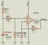
There must be many suitable FET's out there but the J111 and 112 are suitable. Look at the data sheets for the differences in "pinch off" voltage.
Uh-huh")
The inverting or virtual earth opamp configuration has essentially no measurable voltage input at the inverting input. If the series pass FET is placed here (as in my switch) then the series pass FET sees no (or very little) voltage across it. With a 10K input resistor and FET Rds of say 50 ohms then with 10 volts applied to the input only around 50 millivolts appears across the FET.
Because the FET is always very close to having zero volts on it the bias voltages are simple to arrange. With the pass transistor in series with a large voltage output swing (as in yours) then the gate bias has to track or follow the signal by tying the gate and source together with a resistor. As the gate is a high impedance (and so prone to stray pickup) it makes sense to keep the resistor fairly low (22K). To turn the FET off the gate is pulled negative by at least Vgs (dependent on FET) plus the maximum signal voltage that you are trying to block... hence the high negative voltage needed. This problem is much reduced with the virtual earth arrangement as there is no signal voltage on the FET so the turn off voltage can be less.
If you want to keep experimenting with your circuit try something like this although you will get better results using a virual earth amp and doing the switching at the input.
Get the switching right first and then think of slowing it down with an R/C network if needed.
Uh-huh
The inverting or virtual earth opamp configuration has essentially no measurable voltage input at the inverting input. If the series pass FET is placed here (as in my switch) then the series pass FET sees no (or very little) voltage across it. With a 10K input resistor and FET Rds of say 50 ohms then with 10 volts applied to the input only around 50 millivolts appears across the FET.
Because the FET is always very close to having zero volts on it the bias voltages are simple to arrange. With the pass transistor in series with a large voltage output swing (as in yours) then the gate bias has to track or follow the signal by tying the gate and source together with a resistor. As the gate is a high impedance (and so prone to stray pickup) it makes sense to keep the resistor fairly low (22K). To turn the FET off the gate is pulled negative by at least Vgs (dependent on FET) plus the maximum signal voltage that you are trying to block... hence the high negative voltage needed. This problem is much reduced with the virtual earth arrangement as there is no signal voltage on the FET so the turn off voltage can be less.
If you want to keep experimenting with your circuit try something like this although you will get better results using a virual earth amp and doing the switching at the input.
Get the switching right first and then think of slowing it down with an R/C network if needed.
Attachments
Last edited:
boo yah it works! it's alive! The first thing I did was to simulate the circuit. Now I have to mount the prototype (analog switch only).
I didn't think it was that easy, remove leftover components. Now the only question is: how do I add the R/C network? Only to Q1 or Q5 also? I understand that is used as a regular R/C network, ie as it was in the original design, the network formed by R13 and C1. How long time I calculate for switching? Tens of milliseconds? I'm considering to change the analogue supply rails to ±15V, which isn't big deal and I ensure the proper functioning of the shunt FET. Better, right?
Thank you for the explanations given, unfortunately my differents teachers of analog electronics were not too... How can I say? hard-working. I will test J111 for the switch.
I understand that you recommend me reverse the order of the blocks? That is, at device input, switch first and then (input) buffer. It seems strange that recommendation. If that is correct I'd rather not, the idea of the input buffer is not to load the signal from the outside. I must have misunderstood because it hard to believe. You can explain it?
The idea of the operational amplifier I have been considering from the beginning, but to be honest, I prefer to use only discrete components, without any IC (except the control block, which will use a microcontroller). The reason is simply economic, to learn, and may be a whim. I think you can get the same results without op amp at the expense of complicating the circuit and one more headache. But I really LOVE the analog circuits in its purest form. You learn a lot with them, do not you think?
While I play with the prototype of the analog switch (I'll keep you posted), some help to rebuild the buffers? I'm going too far, I know.
Thousands of thanks, I know I'm a bore.
I didn't think it was that easy, remove leftover components. Now the only question is: how do I add the R/C network? Only to Q1 or Q5 also? I understand that is used as a regular R/C network, ie as it was in the original design, the network formed by R13 and C1. How long time I calculate for switching? Tens of milliseconds? I'm considering to change the analogue supply rails to ±15V, which isn't big deal and I ensure the proper functioning of the shunt FET. Better, right?
Thank you for the explanations given, unfortunately my differents teachers of analog electronics were not too... How can I say? hard-working. I will test J111 for the switch.
If you want to keep experimenting with your circuit try something like this although you will get better results using a virual earth amp and doing the switching at the input.
I understand that you recommend me reverse the order of the blocks? That is, at device input, switch first and then (input) buffer. It seems strange that recommendation. If that is correct I'd rather not, the idea of the input buffer is not to load the signal from the outside. I must have misunderstood because it hard to believe. You can explain it?
The idea of the operational amplifier I have been considering from the beginning, but to be honest, I prefer to use only discrete components, without any IC (except the control block, which will use a microcontroller). The reason is simply economic, to learn, and may be a whim. I think you can get the same results without op amp at the expense of complicating the circuit and one more headache. But I really LOVE the analog circuits in its purest form. You learn a lot with them, do not you think?
While I play with the prototype of the analog switch (I'll keep you posted), some help to rebuild the buffers? I'm going too far, I know.
Thousands of thanks, I know I'm a bore.
Good to hear you are getting it to work.
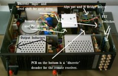
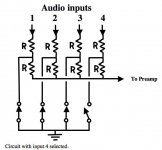
Yes, it's true an inverting stage (as mine) loads the source. For me that is not a problem but I can understand if you do not wish to do that I did it because it allows one buffer to be used for all inputs and the layout lends itself to a compact design where the FET's are right at the input sockets. Also, the virtual earth mixer, which is really what my circuit is, gives much improved crosstalk on the compact PCB layout rather than a non inverting stage. You can see the rows of FET's here.
I agree that building and playing around with discrete circuitry is the best way to learn.
Yes, it's true an inverting stage (as mine) loads the source. For me that is not a problem but I can understand if you do not wish to do that
I did it because it allows one buffer to be used for all inputs and the layout lends itself to a compact design where the FET's are right at the input sockets. Also, the virtual earth mixer, which is really what my circuit is, gives much improved crosstalk on the compact PCB layout rather than a non inverting stage. You can see the rows of FET's here.I agree that building and playing around with discrete circuitry is the best way to learn.
Attachments
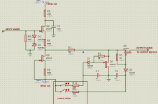
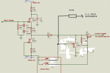
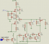
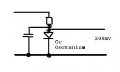
I'm still working, I added the adapter for the logic control inputs and the 200mV reference voltage circuit (190mV on a simulation, will adjust when mounted).
BTW, I've been thinking a lot, I'll use any op amp, until now in the power supply block and perhaps in the output buffer, but no in the input buffer.
I upload screenshots of the new designs. Once I have it mounted I'll tell you more.
Once again, thanks.
BTW, I've been thinking a lot, I'll use any op amp, until now in the power supply block and perhaps in the output buffer, but no in the input buffer.
I upload screenshots of the new designs. Once I have it mounted I'll tell you more.
Once again, thanks.
Attachments
- Status
- This old topic is closed. If you want to reopen this topic, contact a moderator using the "Report Post" button.
- Home
- Source & Line
- Analog Line Level
- Some help with high end input selector.