Addendum: I believe that the turn-on thump, if any, is now cured with the addition of C1 - but I've only tested it in the LF02 + LM6172 and MiniRef, which did not have a turn-on thump at any rate. A similar mod should also work on the LF01 + LM318 in the MyRef Rev C.
R4 @ 93r1 is precise.
Does it need to be that?
Took me a while to work out that e-6 = µ
R4 just has to be reasonably matched across both channels - 1% is fine. I just happened to have 93R1 in RNC55 1% MFR. Anything from ~47 to 100R should be fine, but the quiescent current of the output stage is set by R4 - the higher it is, the lower the Iq.
The mu symbol doesn't always display correctly when exported from an LTSpice schematic, hence scientific notation is safer.
have a question about the schematic in post post 60:
What component should V4 be? Can I just use a diode for the voltage drop?
Yes, it's possible to use diode(s) at V4, and that's what I'm using in my present experiments withe the LF02 (which is basically a dual LF01 with minor differences).
1) With a 1.12V IR LED as V4, R4 can be ~43..51R.
2) With a BAS40-04 (2x Schottky diodes in an SOT23 package), Vf ~= 0.76 V, R4 can be ~8.2..12R.
3) With an 1N4148 + (Chinese) 1N60P in series, Vf ~= 0.94 V, R4 can be ~22..27R.
Is Rs, R1 and R8 necessary when used in the myRev? I assume this is only for simulation purposes.
Yup, only used in simulation - the physical module doesn't have any of Rs, R1, R6 and R8.
BTW, Q1 = 2sc1815-GR (original Toshiba) and Q2/Q3 = NOS metal can 2n2221/2n2905 (or equivalent) seems to give the best subjective sonics so far in an LF02/MiniRef v1.04. This is with an Everbright IR LED for V4 as mentioned above. Not sure why, but metal cans probably have slightly better thermal inertia and keep the die temperature more constant. 2sc1815-GR at Q1 has lower Vceo and should therefore have better quasi-saturation chacteristics than 2sc1845.
Another candidate pair for the output devices is 2sc945/2sa733, especially if you're planning to use it a higher output-stage quiescent current to drive a low-Z load like headphones in a CMoy-like setup. This application is not yet validated.
Thank you Siva, very much apprechiated.
I will design a small PCB according to you layout, if it turns out ok, I will post it here.
I will design a small PCB according to you layout, if it turns out ok, I will post it here.
You're welcome. I would suggest including R6 in the layout - if it is not used, it can be jumpered out, but gives more flexibility for those who want to use both R4 and R6 for symmetrical push-pull operation. Also give several alternate package alternatives for V4 - at the least, SOT23, TO92 and 2x DO35 (vertical) should cover most biasing choices.
Hello,
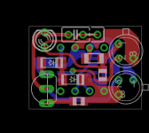
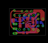
I designed a small PCB for the LF01 with the attached schematic and would be glad for helpful comments.
Included are :
C1: with 5 mm through hole spacing
R6 (R5 in my schematic): 0805 type
C2: filter capacitance 0603 type between rails, as in your early schematics
R4: 1206 type
all other R: 0805 types
Q1: 2SC1815
Q2/Q3: 2n2221/2n2905 as TO18 metal can types
V4: 3mm LED
D1/D2: as SOD123 types
The PCB is roughly 19,5x14,5 mm in size.
Are there any obvious mistakes, or things to improve?
Attachments
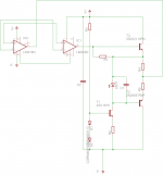
I do not understand your schematic!
Amp inputs tied together ?? Buffer o/p to amp o/p?
Wires very crossed somewhere.
Amp inputs tied together ?? Buffer o/p to amp o/p?
Wires very crossed somewhere.
I do not understand your schematic!
Amp inputs tied together ?? Buffer o/p to amp o/p?
Wires very crossed somewhere.
The LM318N is just used for the pinout to the baseboard-socket and can be ignored. The new daughter board would plug into a LM318 in DIL08.
I could have made that more clear, right.
What is relevant is the output stage following the output of the LM318D.
C1: with 5 mm through hole spacing
R6 (R5 in my schematic): 0805 type
C2: filter capacitance 0603 type between rails, as in your early schematics
R4: 1206 type
all other R: 0805 types
Q1: 2SC1815
Q2/Q3: 2n2221/2n2905 as TO18 metal can types
V4: 3mm LED
D1/D2: as SOD123 types
The PCB is roughly 19,5x14,5 mm in size.
Are there any obvious mistakes, or things to improve?
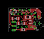
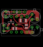
A few suggestions: pins 1 and 5 of the SOIC8 opamp may be brought out to pins 1 and 5 of the DIP8 pins. They aren't used in the MyRef Rev C, but there may be other applications where offset null or alternate compensation pinouts on other single SOIC8 opamps may be needed, e.g. on AD797 or OPA627 or LT1028.
C2 can be made 0805 (which will also allow 0603) as well as 2.5mm through-hole alternate (e.g. Wima FKS02).
D1/D2 can perhaps be combined into one SOT23 package - would allow BAV99 or 1.24V bandgap references to be used instead.
There are also a few placement alterations I would make to allow more easy soldering of SMD components without the risk of solder bridges or shorts.
If all Rs are made 0805, it would also allow the use of 0102 MicroMELFs at the same location as alternates. Similarly, 1206 would allow 0204 MiniMELFs. It's not mandatory, just something to consider.
Q1 can use a smaller footprint for TO92 with pins 1 & 3 spaced 2.54mm apart, and pin 2 offset between 1 & 3. Several transistors are available with the leads already bent for that pinout, but it's not difficult to bend the inline TO92 devices to the smaller footprint at the time of assembly.
Last edited:
Mhh, those were some good remarks. Especially the SOT23 footprint for the diodes and the smaller TO92 footprint liberate a lot of space.
OK, attached is another version.
I am not really satisfied. I wanted to get it smaller, or tidier. Both at best. But this is it.
Soldering would be done under a microscope, so I don´t worry about solder-bridges.
I am not able to connect Pin 1 and 5 to the outside in this version (and size), but for the myMyref I don´t need it.
Probably I will do another larger version that has pin 1 and 5 connected and maybe offers more options. A higher current version as cmoy headphone buffer would be interesting...
Thanks for the help so far 🙂
Attachments

linuxguru: Do you have the balls to make things right for yourself and ship me the PCBs I bought and paid from you several months ago? You have ignored all of my PMs.
Ive built this circuit and it sounds very very good. Now thinking of turning it into a headphone amp with maybe bd139 140. How can i increase the bias substantially for that?
Trying to get back into the diyAudio loop after a long gap - here goes:
For a Headphone amp, it depends on the amount of Class-A bias you'd like in the output stage. 25 mA or higher may run a bit warm, depending on the rail voltages.
The alternate approach is to use a smaller Vf on the biasing diode V4 - for instance, BAS40 (2x Schottky in an SOT23 package) will give about 0.76 V, which will allow the use of smaller emitter-ballast stabilization resistors in the output stage (of the order of a few ohms, say 2x 8.2 ohms).
While not necessarily true Class-A operation, it may be a reasonably trade-off for a headphone amp to go into Class-AB at high swings and let the loop-gain of the opamp fix up the additional distortion.
I was thinking something closer to 200ma and really make the circuit versatile. Does it not make sense to replace the output transistors to something bigger for it?
For 200 mA, you'll need beefier output devices, and maybe bolt-on heatsinks depending on the rail voltages - you may want to drop it to +/- 5 to 6V to keep dissipation manageable. That will also limit your choice of usable op-amps to relatively low-voltage devices - LM6151/6171 may be worth looking at.
Oh i have some very big heatsinks 😀😀
What about the input impedance of q1 tho? Would it affect the sonics substantially if its replaced by a lowly device such as bd139?
What about the input impedance of q1 tho? Would it affect the sonics substantially if its replaced by a lowly device such as bd139?
Last edited by a moderator:
Perhaps you're referring to the output NPN Q2? You'll probably have to measure and select them for moderately high beta of say 100+ - which should not be a problem as BD139 is available with Hfe up to ~150-200. It may droop a bit at 200 mA Icq, though. Hitachi 2sd669/b649 may be an even better choice if you have access to authentic originals - there are a lot of copies floating around.
Current source Q1 may be set to 4-8 mA. If you go much higher, you'll have to worry about dissipation in Q1 also.
Current source Q1 may be set to 4-8 mA. If you go much higher, you'll have to worry about dissipation in Q1 also.
- Home
- Source & Line
- Analog Line Level
- ANN: LF01 Discrete/Hybrid Opamp Module