Hello,
I am struggling to try to find out a principle to apply for a schematic I need. I am studying for a while my hybrid amplifier trying all known typologies. this amplifier is with symetrical input (differential 2 x 12AT7).
My goal is to use differential inputs (XLR) and make a connection to the 12AT7. Unfortunately, the feedback resistors (low for noise) are not compatible with the minimum input impedance for XLR. 10k?
So I investigate a single differential buffer. 2 inputs. 2 outputs. No feedback necessary, thus no room for resistor noise. Or maybe feedback ok, but idea to have optimum noise/input impedance?
I have seen some attempts here and there but no prototpe nor sims were done.
Do you have any guideline? Isn't it a common requirement? I feel not so good to use a 100dB AOP to have a x1 gain. I will go if I have no choice (well, you understand, it is philosophical... my Hybrid has no feedback neither... except final BJT buffer...)
Hope you can help!
best regards
Laurent
I found following document concerning fully differential amplifiers : http://focus.ti.com/lit/an/sloa054d/sloa054d.pdf
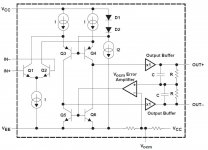
The schematic (attached) is a good starting point for a discrete design.
Back home yesterday evening, I LTspiced a version with +/-50V power supply. First version with current sources, second with resistors instead of current source.
Surprisingly, it is easy to have a low distorsion (lower than ppm) in differential mode with 4 V ouput signal (see application schematic).
Didn't think about coming office with models... no web at home. I will post another day.
I have now a differential buffer that suit half the requirement :
- differential in : ok
- differential out : ok
- gain=1 : ok
- low output impedance : ok
- high input impedance : not yet ok, depends on R1, R3
- low value resistors on signal path : not ok, compromize with previous point
I tried before night to degenerate the circuit to have a buffer without feedback. I have a buffer, but distorsion is not as low... as expected.
Hope you can react on that with your experience?
I would feel bad with 10k resistors for R1...R4, too high the noise. Not you? What about noi
Attachments
If you put a unity gain buffer before each input of your circuit, you can have high input impedance even with low values for R1,2,3 and 4.I have now a differential buffer that suit half the requirement :
- differential in : ok
- differential out : ok
- gain=1 : ok
- low output impedance : ok
- high input impedance : not yet ok, depends on R1, R3
- low value resistors on signal path : not ok, compromize with previous point
If you put a unity gain buffer before each input of your circuit, you can have high input impedance even with low values for R1,2,3 and 4.
That's a way i am investigating. I need just two BJT buffers. Goal would be to have low distorsion ones at a few volts input level. Maybe Emitter follower loaded by a current source?
Will have to investigate that, not a lot of time right now. Will post simulation files ASAP.
I found it. Jfet follower loaded with jfet CS. ok. ".0007% distortion waveform at 1 Volt and 1 kHz." oh. nice.
have to find out if that is ok for DC coupling. no sure about vgs mismatch.
What? I forgot to say that? Yes, all the design is DC coupled from input to output with high voltage 12AT7 on the path (powered at 150V).
Some sparks to be expected. Spice doesn't warn about this.
Maybe some coupling cap on the path one day. Nobody's shocked yet.
BJTs can be used for buffers. They can do an excellent job.
It just happens that the two simplest buffers that came to mind were both jFET input.
Go to Pass site and download the B1 manual.
Go to the DCB1 thread for a DC coupled version of the B1.
There is also a thread or two about using the BF862 as a buffer as well as a +gain amplifier.
It just happens that the two simplest buffers that came to mind were both jFET input.
Go to Pass site and download the B1 manual.
Go to the DCB1 thread for a DC coupled version of the B1.
There is also a thread or two about using the BF862 as a buffer as well as a +gain amplifier.

this is not quite right.I got it. I matched jfet with same temp and same id, then same vgs.
Possible without matching by hand..?
The definition of Idss is that Vgs = 0volts and Vds = 10Volts and Tj= 25degC, then the current that flows is Idss.
Now turn that definition around and apply a Vds = 10Volts, pass an Id exactly equal to that device's Idss and provided Tj = 25degC then Vgs will be zero volts.
That's the beauty of the B1.
Pick two jFETs with the same Idss.
Use one as a Constant Current Sink (CCS).
The CCS will allow the follower to pass Id=Idss. Then Vgs of the follower is 0volts.
When Vgs is 0volts, that tells you and I that the voltage at the gate is exactly the same as the voltage at the Source.
Apply 0Vac to the Gate and the output, at the Source, is 0Vac
Apply 102mVdc to the Gate and the output is 102mVdc.
Apply 1Vac to the Gate and the output is 1Vac.
In other words the CCS loaded jFET acts as a unity gain follower/buffer.
But as with any Follower/buffer the current at the input is not the same as the current at the output. In general Buffers use tiny input current to generate large output current, they are current amplifiers.
Ok for definition of Idss (I don't use often the equation, I work mainly with bjt).
But if we work the current source with vgs<>0, this vgs will also be the offset of the buffer no? (because upper fet will need same vgs for same Id)?
Idss and vgs=0 are not only a specific case to have zero offset?
Is vgs=0 required even if DC offset is of no importance? (wonder why it is used on B1 with 2 coupling cap)
The B1 uses a single supply.
It uses, as do all amps that run at elevated voltages, capacitors to block DC and allow AC signals to pass.
The DCB1 uses a dual polarity supply and relies on the follower running at Idss for it's IC to generate no DC output offset of it's own.
It run at voltages around the signal return voltage and thus does not need DC blocking caps to operate.
Because the DCB1 is DC coupled it will pass DC from a Source to a Receiver.
The B1 is AC coupled.
I don't understand what you are trying to tell/ask us.But if we work the current source with vgs<>0, this vgs will also be the offset of the buffer no? (because upper fet will need same vgs for same Id)?
Hi,
when You use matched JFETs and sysmmetrical power supplies, give the sourcefollower-JFET the same source resistance as the currentsource-JFET and the offset will be 0. In any different case the offset will be off of 0.
Because of the gm not beeing infinite, the gain of the follower will be less than 1 (>0.9), with lower gm-values resulting in lower values.
You may also think about cascading high-gm/low-Ugs JFETs with lower-gm/high-Ugs devices to achieve a gain very closely to 1, to get a low output impedance value, to deal with heat-/power-problems and to avoid Udg possibly becoming too high.
The reason for running the JFETs at Idss is that Idss is the maximum current a single-ended ccs-loaded circuit running in class-A can provide into the load. But if Your load current requirements are modest it might be advantageous to use source resistors and run the JFET on a lower-than-Idss current value and enjoy the less stringent requirement for matching tolerance. Alternatively You could modify the constant current source into a voltage controlled current source, which would allow for higher-than-Idss currents into the load.
jauu
Calvin
Last edited:
Thank you for your advises.
Last week, before going holidays, I tried to simulate all that in a first try. I am almost satisfied of the results of this.
To summurize :
Differential output :
- THD20 20Vpp : 0.0022%
- THD20 4Vpp : 0.000082%
- THD20 1Vpp : 0.000005%
Differential buffer output
- THD20 20Vpp : 0.002067%
- THD20 4Vpp : 0.000075%
- THD20 1Vpp : 0.000005%
I didn't have time to optimize the circuit to improve non-differential performances, it seems different values must be used if we need differential use or not.
Some comments on the schematic :
- I draw it as a super-symetric-differential-buffer just for artistic reasons. Find the part that are not differentials...
- +/-24V is used to allow high ouput swing and rather good linearity with resistors replacing current sources.
- Q19, Q20 are input buffers. I didn't use Jfet as I don't really mind about offset (and as I think any BJT is already matched for this application compared to JFET), the differential buffer will remove it. I just need a good buffer and gm of BJT may do the job.
- Q21, Q22 are the emiter source current for input buffer. Need to be optimized for high input level and low load resistors (Ra, Rb)
- Q17, Q18 is the differential pair of the previous schematic posted. Current source has been removed to simplify and replaced by R26
- Q15, Q16 is the cascode pair of previous schematic. Current sources have been replaced by R24, R25 to simplify. Base voltage is controled by Q1 to eliminate output offset (more on this later)
- Q14, Q13 is output buffer, R20, R21 are low to allow high swing in low ouput impedance (10Vpp on 1k is ok) (have to think about power dissipation for Q13, Q14)
- Q1, Q2 is a differetial pair that controls ouput offset. Voltage is sensed using R34, R35.
- C5, C6 have not been optimized (did no loop gain/phase simulation). First try values as a guess.
- I just played with available components in standard versions.
- Playing with temperature didn't help to optimize ouput offset, it stays to -27mV due to matched models...
This is all I will provide today, I am back to work and have to do some job...
I hope my first circuit contribution to DIYaudio will be received indulgently.

Any comment welcome! (on schematic or LTspice use...)
Last week, before going holidays, I tried to simulate all that in a first try. I am almost satisfied of the results of this.
To summurize :
Differential output :
- THD20 20Vpp : 0.0022%
- THD20 4Vpp : 0.000082%
- THD20 1Vpp : 0.000005%
Differential buffer output
- THD20 20Vpp : 0.002067%
- THD20 4Vpp : 0.000075%
- THD20 1Vpp : 0.000005%
I didn't have time to optimize the circuit to improve non-differential performances, it seems different values must be used if we need differential use or not.
Some comments on the schematic :
- I draw it as a super-symetric-differential-buffer just for artistic reasons. Find the part that are not differentials...
- +/-24V is used to allow high ouput swing and rather good linearity with resistors replacing current sources.
- Q19, Q20 are input buffers. I didn't use Jfet as I don't really mind about offset (and as I think any BJT is already matched for this application compared to JFET), the differential buffer will remove it. I just need a good buffer and gm of BJT may do the job.
- Q21, Q22 are the emiter source current for input buffer. Need to be optimized for high input level and low load resistors (Ra, Rb)
- Q17, Q18 is the differential pair of the previous schematic posted. Current source has been removed to simplify and replaced by R26
- Q15, Q16 is the cascode pair of previous schematic. Current sources have been replaced by R24, R25 to simplify. Base voltage is controled by Q1 to eliminate output offset (more on this later)
- Q14, Q13 is output buffer, R20, R21 are low to allow high swing in low ouput impedance (10Vpp on 1k is ok) (have to think about power dissipation for Q13, Q14)
- Q1, Q2 is a differetial pair that controls ouput offset. Voltage is sensed using R34, R35.
- C5, C6 have not been optimized (did no loop gain/phase simulation). First try values as a guess.
- I just played with available components in standard versions.
- Playing with temperature didn't help to optimize ouput offset, it stays to -27mV due to matched models...
This is all I will provide today, I am back to work and have to do some job...
I hope my first circuit contribution to DIYaudio will be received indulgently.
Any comment welcome! (on schematic or LTspice use...)
Attachments
I proposed to run Jfets at lower Id than Idss. For this, Vgs will need to be modified (Vgs<>0) and then offset appear.I don't understand what you are trying to tell/ask us.
As Calvin said, no real added value, maximum current is best for buffer.
The idea behind this was not to use Jfet running with Vgs=0, but using BJT with Vbe=0.7V. The end of the idea is the schematic posted above. As you see on schemtic, I can manage input buffer offset in another way.
- Status
- This old topic is closed. If you want to reopen this topic, contact a moderator using the "Report Post" button.
- Home
- Source & Line
- Analog Line Level
- Differential buffer without feedback?