This is a further development of the ideas in this thread:
http://www.diyaudio.com/forums/soli...-super-pair-buffer-simulation-schematics.html
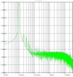
The schematic shown is a conceptual/simulation schematic of a 2-stage buffer consisting of an input LTP stage, followed directly by the low-distortion buffer from the thread above. The LTP uses a bootstrapped floating current mirror (a la AD797), and also a bootstrapped floating current source using ideas from Russ White's Diamante Headphone amp. The overall circuit uses only 10 BJTs to achieve THD20 of -120 dB at 1V amplitude into 32 ohms - probably one of the simplest circuits with this level of performance. Almost all the BJTs are jelly-bean types or can be substituted by jelly-bean types without significant impact on distortion.
http://www.diyaudio.com/forums/soli...-super-pair-buffer-simulation-schematics.html
The schematic shown is a conceptual/simulation schematic of a 2-stage buffer consisting of an input LTP stage, followed directly by the low-distortion buffer from the thread above. The LTP uses a bootstrapped floating current mirror (a la AD797), and also a bootstrapped floating current source using ideas from Russ White's Diamante Headphone amp. The overall circuit uses only 10 BJTs to achieve THD20 of -120 dB at 1V amplitude into 32 ohms - probably one of the simplest circuits with this level of performance. Almost all the BJTs are jelly-bean types or can be substituted by jelly-bean types without significant impact on distortion.
Attachments
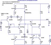
The LTP uses a bootstrapped floating current mirror (a la AD797), and also a bootstrapped floating current source using ideas from Russ White's Diamante Headphone amp..
Sorry, but neither are CCSs, they are series voltage regs, as you are taking the output off the low impedance emitters.
Unless it's a drawing mistake...
Regards, Allen
Sorry, but neither are CCSs, they are series voltage regs, as you are taking the output off the low impedance emitters.
The transistors Q3 and Q12 are bootstrapped voltage sources, for sure. However, R3 in series with the emitter of Q3 ensures that it is a CCS. It is a CCS, because bootstrapping of the base of Q3 from the output (through the zener) ensures that the emitter of Q3 is a level-shifted version of the output. Similarly, the other end of R3 also swings as a level-shifted version of the input. Hence the current through R3 is almost constant, and it is a CCS.
The lower bootstrap through Q12 removes the Early Effect on Q1, Q4 and Q5, by making the current mirror float - this is similar to the AD797.
There's no drawing mistake.
Last edited:
The missing connecting dots are an artifact of the .wmf files produced by LTSpice running under Wine/Linux. I get around it by showing unconnected crossings as dog-legs 'jumping' over the other wire - there are 2 of these on this schematic. All other wire crossings are actual connections.
...QUOTE]
Hi Linuxguru!
Do you think this would drive my 16 ohm hp Senheiser cx-400?
Do you think this would drive my 16 ohm hp Senheiser cx-400?
Sure - however, this is just a conceptual schematic. Any real circuit based on this will need some circuit elaborations, additions, compensation tweaks, etc. to make it stable, repeatable and practical.
To drive a 16-ohm headphone with approximately the same voltage swing of 1V peak is conceptually feasible, but may need some component tweaks - in particular, the output-stage load resistor R11 may need to be made smaller to increase the quiescent current in the output stage to keep it out of clipping.
This is a further development of the ideas in this thread:
Almost all the BJTs are jelly-bean types or can be substituted by jelly-bean types without significant impact on distortion.
An admirable goal. I like this basic idea but have not examined it at length.
impressed, but...
again
class A rules
Al Gore is mad again more current to drive, more heat
I guess that putting big ccs instead of r11
and putting output transistors bigger makes power amplifier (buffer) from this circuit.
As impressed me of simulation results, I am thinking that first the signal was amplified then corrected in gnfb, then hf compensated...generally at first was spoiled, at the end was corrected/restored
still looking for good nongnfb ab-class buffer...
...but may need some component tweaks - in particular, the output-stage load resistor R11 may need to be made smaller to increase the quiescent current in the output stage to keep it out of clipping.
again
class A rules
Al Gore is mad again
more current to drive, more heatI guess that putting big ccs instead of r11
and putting output transistors bigger makes power amplifier (buffer) from this circuit.
As impressed me of simulation results, I am thinking that first the signal was amplified then corrected in gnfb, then hf compensated...
generally at first was spoiled, at the end was corrected/restoredstill looking for good nongnfb ab-class buffer...
- Status
- This old topic is closed. If you want to reopen this topic, contact a moderator using the "Report Post" button.
- Home
- Source & Line
- Analog Line Level
- Low-distortion Class-A line/headphone buffer