Nice job done Nick,
You have some nice components on that board
Just make sure it’s not on for long without adequate sinking.
")
Thanks John, good eye. I will have it mounted it later today, after some turkey.
Any one have any idea what is the problem..? Would the negative offset have caused any damage to the amplifier?I measured the offset and the absolute values are good, but then i realized something weird - the faulty channel's offset is negative. Maybe it was negative all this while and i didn't realize it.
when the DCB1 has the correct pair of jFETs the output offset should be 0.0mVdc or slightly negative, eg. -0.9Vdc.
It should not be a +ve output offset.
+ve output offset tells us that the amplifiying jFET (Follower) is operating at >100%Idss.
This can be corrected by swapping around the CCS FET for the Follower FET
It should not be a +ve output offset.
+ve output offset tells us that the amplifiying jFET (Follower) is operating at >100%Idss.
This can be corrected by swapping around the CCS FET for the Follower FET
Thank you, Andrew! I checked it again and you're right - the faulty channel has a +ve offset. I wish i knew more about the circuit, which is the CCS and which is the follower? It's weird cos i'm pretty sure i put in the matched quad FETs that i bought from Ed in the right place. Must have messed up somewhere
You probably didn't mix them up. To find the pair orientation one must test them.
Selecting for Idss is sufficient for B1 and DCB1, but the simple Idss test is not accurate enough if you are looking for pair matching.
Set up a plug board.
Get ready to apply 20V,0V to it.
Connect one of the selected pair as a CCS, i.e. short Gate to Source.
Connect 0V to this Source/Gate
Connect the other with 1k (or 100r) across Gate to source.
Connect it Source to CCS Drain
Connect +20V to the top Drain.
Measure the voltage across the 1k0 resistor. Black probe to Source end and red probe to Gate end. This measurment is the Vgs of the upper device and should be very close to 0.0mVdc. If there is a small offset, this is th eoutput offset of the DCB1.
If the Vgs is +ve then you have the order as required to go into the DCB1. If the Vgs is slightly +ve, then swap the two FETs around. The Vgs should now be slightly -ve. This is the order they get fitted into DCB1.
As an alternative solder a 6pin 0.1" pitch SIL socket into the DCB1. Now you can test on the DCB1 PCB and at the Voltages of the DCB1.
I'm sure Andrew is absolutely correct, but I am pretty sure that many DCB1's have *small* negative or positive offsets. Cersepn seems to have a condition where one channel is not working. The polarity of a small offset voltage would not break the DCB1 nor a following amplifier. Most builds using matched jfets have offset magnitudes on the order of a few millivolts. If the offset is small, polarity doesn't matter in terms of the circuit actually working. If the offset is large (say >500mV) then polarity doesn't matter, because something isn't working right, and if the following amplifier is DC coupled the offset could cause damage to the power amp.
In short, offset polarity is much less important than magnitude.
In short, offset polarity is much less important than magnitude.
Thank you both, Andrew and nezbleu. So the question that puzzles me is, since the offset magnitude is low, why would the amplifier channel die (again)? The first time round it died because i unplugged a live RCA, but this time round i didn't do anything strange.
The dcb1 + amp pairing worked well for an entire day, yet the next day one amp channel died. I made sure the powering up/down sequence was correct as well, this time being much more careful. So, what gives?
The dcb1 + amp pairing worked well for an entire day, yet the next day one amp channel died. I made sure the powering up/down sequence was correct as well, this time being much more careful. So, what gives?
I once sent a static shock through my system. Can't recall exactly but I think I touched the tuner ON/OFF button and the spark from my finger created a loud noise from the speakers.
One of the 4 jFETs in the buffer section of the DCB1 was damaged.
Initially it gave out a bad offset.
I disconnected the powered up buffer and in the intervening days, the jFET appeared to have repaired itself. The DC offset was very much lower and when connected to the system again the damaged channel appeared to work (in passing audio signal) just as well as the undamaged channel. I continued using it that way for some months to see if the damage got worse. No. it remained about the same, the big offset never returned. The small (damage induced) offset did remain but wandered very slightly compared to the good channel.
That's interesting, so it's possible my jfets might be damaged, hmmm. Yet the offset values are good (<+/- 5 mV). Does it make sense if the amp is sensitive only to + offset? The persistently faulty amp channel is always the one connected to the dcb channel with + offset.
I could get the amp fixed again but honestly am too afraid to use the dcb1 with the amp again.
Is it possible that the repair job wasn't done properly the first time round? Any other advice/suggestions is much appreciated...
I could get the amp fixed again but honestly am too afraid to use the dcb1 with the amp again.
Is it possible that the repair job wasn't done properly the first time round? Any other advice/suggestions is much appreciated...
I don't know who did your "repair job".
I suspect the "repairer" simply swapped out the suspect devices and did not know about the Idss selection requirement.
A service Technician needs information to carry out service. If there is no Service Manual, then where does the Technician obtain his information?
I suspect the "repairer" simply swapped out the suspect devices and did not know about the Idss selection requirement.
A service Technician needs information to carry out service. If there is no Service Manual, then where does the Technician obtain his information?
I'm confused. I thought the Idss selection requirement is only for the dcb1.. ? Is there another Idss requirement for the amp?I don't know who did your "repair job".
I suspect the "repairer" simply swapped out the suspect devices and did not know about the Idss selection requirement.
A service Technician needs information to carry out service. If there is no Service Manual, then where does the Technician obtain his information?
According to the shop owner, they didn't have the service manual, and since the amp circuit's quite complicated, the technician relied on the working channel to diagnose the problem. If i'm not mistaken the only parts that were replaced were a handful of diodes and resistors, nothing big. The problem was with the input stage, output was perfectly alright.
Can I say with a reasonable amount of certainty that it wasn't the dcb1 that killed the channel this time? Not too sure what i should do right now. Should i PM john curl and ask him for his advice since it's his creation?
Cer,
are we at crossed purposes?
The DCB1 is a very simple circuit. Just 1pr jFETs and a few resistors per channel.
Or are you talking about the Power Amplifier being repaired?
The Idss selection is all that is required for the 4 buffer jFETs.
But most who measure jFETs for Idss cannot achieve the required repeatability in measurement. I certainly can't.
That's why when I find a possible selected pair I pair match together to try to reduce the margin of error and get a close Idss pair. It is the very close Idss that results in the near zero output offset.
The alternative is using Feucht, but then we don't have a Pass B1.
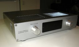
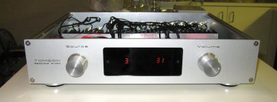
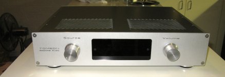
A 'sort of' hotrodded DCB1 build
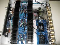
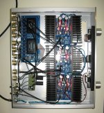
Howdy everyone, attached are some pics of a build of DCB1s. Many thanks to Salas, Tea-Bags and Ed (L) for making this possible.
I used Mez boards, cut down, and hot rodded as the buffers. Sorry for the bastardisation Salas, I did this before I knew there was another option...
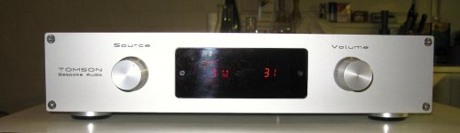
I built it for my Brother who already had the optical volume control system for about the last 12 months, had it mounted on some plywood with leads hanging off it. He drives powered studio monitors (AC coupled) from balanced sources (vinyl and digital), so a balanced volume control makes sense. He likes the one in the pics and has tried others - to be honest I did not hear a massive difference with different optical volume systems. The one in the pics is from here: P&S TECHNOLOGIES INC., and I had the case made by Front Panel Express.
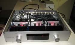
There are three sets of outputs, all in parallel; one balanced set for the main outs, L & R balanced outs for subwoofers, and L & R unbalanced out for a headphone amp.
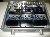
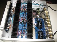
The buffers for the main outs are running at about 580mA, and the heatsinks are running a little over 40 degrees C (25 degrees ambient). The third (butchered) Mez board is running at about 350mA current, and it is powering the unbalanced buffers (on the same board), and also the optical volume system and an additional 4 DCB1 buffers on the matrix board near the power inlet - you can see the wires powering this coming off the regulator output pins (a nice touch on the boards - thanks Salas). The transformer is a 500VA torroid in a separate box, visible in some of the pics.
The offsets are all in the 0-3mV range, with the main outs about 0 to -1.5mV each leg (very low balanced offset). They don't seem to drift much as it all warms up. Also, the LEDs inside sining out of the ventilation slots make it look like a Christmas celebration!
We plugged it in last night - it sounds absolutely fabulous. My brother says his system has never sounded so good, the black background, low level detail and broad soundstage - he's ecstatic about the improvement and I thought it sounded damned good, better detail and smoother than without the buffers.
Thanks again to all,
bk
Howdy everyone, attached are some pics of a build of DCB1s. Many thanks to Salas, Tea-Bags and Ed (L) for making this possible.
I used Mez boards, cut down, and hot rodded as the buffers. Sorry for the bastardisation Salas, I did this before I knew there was another option...
I built it for my Brother who already had the optical volume control system for about the last 12 months, had it mounted on some plywood with leads hanging off it. He drives powered studio monitors (AC coupled) from balanced sources (vinyl and digital), so a balanced volume control makes sense. He likes the one in the pics and has tried others - to be honest I did not hear a massive difference with different optical volume systems. The one in the pics is from here: P&S TECHNOLOGIES INC., and I had the case made by Front Panel Express.
There are three sets of outputs, all in parallel; one balanced set for the main outs, L & R balanced outs for subwoofers, and L & R unbalanced out for a headphone amp.
The buffers for the main outs are running at about 580mA, and the heatsinks are running a little over 40 degrees C (25 degrees ambient). The third (butchered) Mez board is running at about 350mA current, and it is powering the unbalanced buffers (on the same board), and also the optical volume system and an additional 4 DCB1 buffers on the matrix board near the power inlet - you can see the wires powering this coming off the regulator output pins (a nice touch on the boards - thanks Salas). The transformer is a 500VA torroid in a separate box, visible in some of the pics.
The offsets are all in the 0-3mV range, with the main outs about 0 to -1.5mV each leg (very low balanced offset). They don't seem to drift much as it all warms up. Also, the LEDs inside sining out of the ventilation slots make it look like a Christmas celebration!
We plugged it in last night - it sounds absolutely fabulous. My brother says his system has never sounded so good, the black background, low level detail and broad soundstage - he's ecstatic about the improvement and I thought it sounded damned good, better detail and smoother than without the buffers.
Thanks again to all,
bk
Attachments
-
 front-side1.jpg119 KB · Views: 486
 -
 front-top-off2.jpg173.3 KB · Views: 482
 -
 ibternal 2.JPG277.6 KB · Views: 479
 -
 internal 1.JPG330.2 KB · Views: 470
 -
 internal3.JPG315 KB · Views: 467
 -
 internal4.jpg389.6 KB · Views: 324
 -
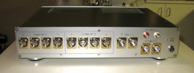 rear1.jpg120.8 KB · Views: 328
 -
 front4.jpg73.6 KB · Views: 276
 -
 front5.jpg105.5 KB · Views: 201
 -
 front6.jpg90.5 KB · Views: 173
This looks awesome! Congratulations on very professional build!
What do you use for displaying volume?
The optical volume system my brother had already comes with it - I just had to supply power and give it a front panel. It connects with the ribbon cable you can see in the pics.
Bkdog,
could you write up a detailed article or Thread explaining each of the stages in that build?
Hi Andrew,
"Detailed" in the way you mean it is probably well beyond me now... This has been about an 8-10 month project. I did keep some notes, but basically I relied on the more experienced players in these forums.
The optical volume board and control board was pre-existing, but I realised that with the impedances involved buffers were needed.
After searching DiyAudio, I then went off and got the wrong board (Mezmerize), but it has made little difference.
I built the standard buffers, using Caddock resistors for the signal chain (my brother's choice, but I didn't tell him about the TXZ parts because they are about impossible to find in Australia).
I matched the FETs myself from a bag of 100 or so, the signal fets were in the recommended 7-8mA IDSS range, and I matched them pretty carefully because I wanted the offset to be low.
I got the heatsinks from Conrad, mounted them on the buffers, and then started playing with hotrodding them. This led to me noticing that the diodes were getting hot! Salas recommended that I sway them to something beefier, so I used TO220 cased fast versions. They still get warm, but only to about 45 degrees C.
I played with measuring the voltage drop across the current setting resistors and changing it, while watching the heat on the MOSFETS, heatsinks and other devices - eventually settling on the almost 600mA currently in use. It's a dynamic system, so you need to keep measuring and changing / trimming the resistors (there are some under the boards). I think you mentioned this in the thread - so thanks for that tip!
The inputs to the "amplifier" (I have problems with that term on a maximum unity gain box) are connected to the optical volume board. It handles input switching and volume. You can probably see this from the pics. The outputs of this board go to the buffers.
The input impedances of the buffers were tripled (a tad more actually) as they are in parallel. The unbalanced output is driven from the hot output of each channel and there is an extra resistor on the cold side to keep the impedances as balanced as possible. The buffer on the RHS (looking at the front) drives the hot and cold legs of the left output, the next board across drives the hot and cold of the right output and the left hand buffer (not as hotrodded as the others) drives the unbalanced headphone outs as well as supplying power for the volume board and the separate buffers for the subwoofer outs (output 3 on the rear panel).
There may be some arguments that this does not fully satisfy the specification for balanced operation - so it goes, I don't really care, it matches the system it's built for and it sounds super (thanks again guys).
The biggest problem was that my brother bought some bloody expensive, flat, cotton-covered silver wire to wire it all up with - it is a PITA to use! It's all of the black wire in the point-to-point wiring in it. It's inflexible, difficult to strip, and hard to solder because it's big and a bit springy... Anyway, it's done now and I hope I don't have to touch it again.
Hope that helps,
bk
- Home
- Source & Line
- Analog Line Level
- Salas hotrodded blue DCB1 build