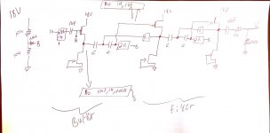
![WP_20150311_001[1].jpg](/community/data/attachments/418/418417-72de8e7d6ff579bc9051b675cdacbaba.jpg)
Finished my 2 way active xover")
Looks Good!
How does it sound??
Hi AndrewT and other guys
I have open baffle speaker (FR and SUBWOFFER) and want to build 2 way crossover. (DAC > B1 > filter > F5)
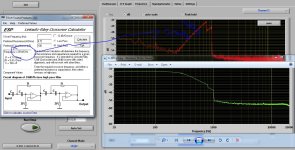
Start with Linkwitz-Riley 24DB/DEC base on OP and its look Great (200Hz).
Now i want to replace the OP with B1 (Nelson Pass).
i tray to understand where to connect the C,R (Linkwitz-Riley scheme(exemple picture)) to the B1 scheme.
What about the C201 cap, do i need it in the filter stage? or just in the output buffer? same about theR204,R205,C200,R202 (i dont need the POT).
Try to mix with the scheme that AndrewT publish here
Thanks
I have open baffle speaker (FR and SUBWOFFER) and want to build 2 way crossover. (DAC > B1 > filter > F5)
Start with Linkwitz-Riley 24DB/DEC base on OP and its look Great (200Hz).
Now i want to replace the OP with B1 (Nelson Pass).
i tray to understand where to connect the C,R (Linkwitz-Riley scheme(exemple picture)) to the B1 scheme.
What about the C201 cap, do i need it in the filter stage? or just in the output buffer? same about theR204,R205,C200,R202 (i dont need the POT).
Try to mix with the scheme that AndrewT publish here
Thanks
Attachments
Last edited:
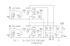
C210 is the DC blocker that has been added to the B1 output.
If there is another DC blocker then you don't need a second.
The F5 is DC coupled. It does not have a DC blocker.
So somewhere between the Crossover filters and the F5 input you need a DC blocker. Choose where you want that, In the crossover or in the F5.
For me, putting the DC blocker inside the F5 is safer. That allows me to connect anything and not blow up my speaker/s.
C200 is the input DC blocker.
You need that before you attach anything to the B1 input.
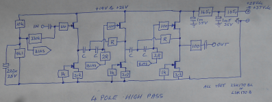
Note the first stage of the second diagram.
That first stage is a B1 with an extra 2r2 source resistor.
Note also that this first stage has an input DC blocker just after IN and has an output DC blocker (C) as part of the Butterworth HP filter.
It is useful to note that EVERY stage of the HP filter has a DC blocker at INput and at OUTput.
This does not happen with a cascade of LP filters. Any DC fed in at the beginning accumulates with any DC offset generated by any of the stages.
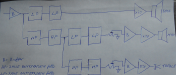
Note in the 4th diagram that the LP filter does not have a DC blocker. You must not pass a DC bias into that LP filter.
The HP filter does have the required DC blocker.
If there is another DC blocker then you don't need a second.
The F5 is DC coupled. It does not have a DC blocker.
So somewhere between the Crossover filters and the F5 input you need a DC blocker. Choose where you want that, In the crossover or in the F5.
For me, putting the DC blocker inside the F5 is safer. That allows me to connect anything and not blow up my speaker/s.
C200 is the input DC blocker.
You need that before you attach anything to the B1 input.
Note the first stage of the second diagram.
That first stage is a B1 with an extra 2r2 source resistor.
Note also that this first stage has an input DC blocker just after IN and has an output DC blocker (C) as part of the Butterworth HP filter.
It is useful to note that EVERY stage of the HP filter has a DC blocker at INput and at OUTput.
This does not happen with a cascade of LP filters. Any DC fed in at the beginning accumulates with any DC offset generated by any of the stages.
Note in the 4th diagram that the LP filter does not have a DC blocker. You must not pass a DC bias into that LP filter.
The HP filter does have the required DC blocker.
Last edited:
Thanks Andrew
The first stage is pure B1, i remove the C201, R204, R205 from it.
Second stage: remove the R202, C200, and C201, R204, R205.
Third stage: remove the R202, C200.
I appreciate if you have a look at the scheme above.
do i need 1K (R202) in Second stage&Third stage before the gate?
The first stage is pure B1, i remove the C201, R204, R205 from it.
Second stage: remove the R202, C200, and C201, R204, R205.
Third stage: remove the R202, C200.
I appreciate if you have a look at the scheme above.
do i need 1K (R202) in Second stage&Third stage before the gate?
Attachments
Pass has not shown gate stoppers.
My diagram played safe and did include gate stoppers.
If you adopt gate stoppers they MUST be attached to the Gate and preferably with a short lead.
I have shown a resistor between Bias voltage and every receiver follower.
You have the one resistor feeding all the stages, but only two have their own resistances.
Last edited:
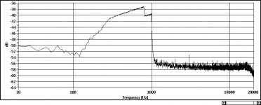
Hi
i build the first stage filter and the second stage (no buffer for now). connected the PC sound card to the firs cap C.
First measure the IDSS for the 2sk246: ~2mA |Vgs=0, Vcc=18v (in the datasheetis 8-12mA)
the Vgs is 0.05v, when output connect to GND trough resistor.
Vgs=0.7, when Vout=GND
Vout before the 10uf cap is 9Vdc
Av: Vin=1.6, Vout=750mV why?
Measurements:
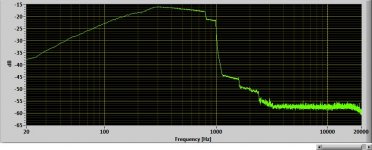
The sweep is 1-900Hz
You can see the first and the second stage.
But why the crossover frequency is shift? in the pic the f is~500Hz, in the calculator is 240Hz ( the LPF in the pic is with OP amp)
Thanks
i build the first stage filter and the second stage (no buffer for now). connected the PC sound card to the firs cap C.
First measure the IDSS for the 2sk246: ~2mA |Vgs=0, Vcc=18v (in the datasheetis 8-12mA)
the Vgs is 0.05v, when output connect to GND trough resistor.
Vgs=0.7, when Vout=GND
Vout before the 10uf cap is 9Vdc
Av: Vin=1.6, Vout=750mV why?
Measurements:
The sweep is 1-900Hz
You can see the first and the second stage.
But why the crossover frequency is shift? in the pic the f is~500Hz, in the calculator is 240Hz ( the LPF in the pic is with OP amp)
Thanks
Attachments
Last edited:
Hi,
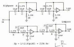
compare sketch no2 and schematic no4 in #248.
They are not the same, but no2 contains important differences.
Sketch the filter circuit first after example no4 and then think where to put the bias.
You see the difference regarding impedance values between the Bias points and gnd?
Also, include gate resistors ... 100R will suffice.
jauu
Calvin
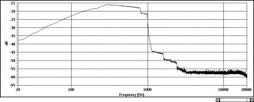
Hi
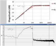
I Start with the schematic no4 with OP, then i change to sketch no2, the value for the filter was the same, 4K7,200nF. (240Hz)
i start with B1 like in post #250 scheme, and then add all the resistor from sketch no2.
Finely I finish with sketch no2, (only no buffer, PC direct to the first filter cap)
Thanks about the IDSS info, this fet its only for test, i will move to 2sk117-bl.
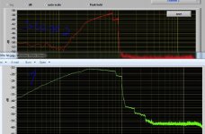
The plots are only frequency response for the first and second stage. (0-900Hz Sweep)
Just want to be sure the results are good and build the circuit.
Calvin: i don't understand, the OP (schematic no4 )is not equal to the B1 for example?
My goal is to replace the OP in the LR filter with discrete amplifier like the B1, I'm wrong?
edit: in the LR filter the 2R connected to GND, here its Bias.
I really impressed from the LR filter (base OP), just want to change the OP
thanks
I Start with the schematic no4 with OP, then i change to sketch no2, the value for the filter was the same, 4K7,200nF. (240Hz)
i start with B1 like in post #250 scheme, and then add all the resistor from sketch no2.
Finely I finish with sketch no2, (only no buffer, PC direct to the first filter cap)
Thanks about the IDSS info, this fet its only for test, i will move to 2sk117-bl.
The plots are only frequency response for the first and second stage. (0-900Hz Sweep)
Just want to be sure the results are good and build the circuit.
Calvin: i don't understand, the OP (schematic no4 )is not equal to the B1 for example?
My goal is to replace the OP in the LR filter with discrete amplifier like the B1, I'm wrong?
edit: in the LR filter the 2R connected to GND, here its Bias.
I really impressed from the LR filter (base OP), just want to change the OP
thanks
Attachments

Last edited:
They don't look like any 4pole filter plots I have ever seen !........................
The plots are only frequency response for the first and second stage. (0-900Hz Sweep)
Just want to be sure the results are good and build the circuit.
the unity gain amplifier block is the same as a B1. That is why we can use a B1 or any simple Follower in that position.Calvin: i don't understand, the OP (schematic no4 )is not equal to the B1 for example?
Bias is connected to Ground via the big capacitor in parallel to 9k1.My goal is to replace the OP in the LR filter with discrete amplifier like the B1, I'm wrong?
edit: in the LR filter the 2R connected to GND, here its Bias.
- Status
- This old topic is closed. If you want to reopen this topic, contact a moderator using the "Report Post" button.
- Home
- Source & Line
- Analog Line Level
- JFET Active Crossover