Thanks Andrew, just for fun attached pic with one channel two way xover (HP+LP) I soldered sockets to change easily the resistors but once known the value I soldered directly the resistor to the pcb, I will start the xover frecuency point with 1kHz, drivers are: tweeter Seas Millenium TCF002 & ScanSpeak 18W-8545-00 (attachd both data sheets), what do you think?
Attachments
![WP_20150117_001[1].jpg](/community/data/attachments/417/417598-a56855c121786021556a6ddaad14dd70.jpg)
why do you need 450mA?
A transformer feeding a capacitance input filter needs an AC current rating at least twice your continuous DC demand, preferably four times.
If you really need 450mAdc continuously, then I recommend 1.8Aac rating.
I have posted this recommendation many times before.
Some can't be bothered reading my posts, don't you?
A 2pole filter requires just one jFET buffer.
Add on an input buffer to feed two 2pole filters and you get somewhere around 6mA to 15mA per crossover.
You can't get much current through the 220r source resistor.
quite different from a k170 with a 2r2 source resistor where you could have 6mA to 10mA per Buffer.
Add on an input buffer to feed two 2pole filters and you get somewhere around 6mA to 15mA per crossover.
You can't get much current through the 220r source resistor.
quite different from a k170 with a 2r2 source resistor where you could have 6mA to 10mA per Buffer.
Those Vgs voltages seem to be far too high.
What devices are you using for the source follower and the CCS in each Buffer?
What is the DC voltage at the output of each Buffer? Is it near the mid point of the supply voltage?
What is the Bias Voltage set up by the two bias resistors?
What devices are you using for the source follower and the CCS in each Buffer?
What is the DC voltage at the output of each Buffer? Is it near the mid point of the supply voltage?
What is the Bias Voltage set up by the two bias resistors?
is 13.5V your gate bias voltage?
Is your supply ~28V?
is 13.9V the voltage after three Buffers?
What are the three output voltages at the Buffer outputs?
Draw a sch and add the voltages.
Something is not adding up.
I can't see from your numbers how
13.9V -13.5V = three times Vgs of 2.04 to 2.64Vgs.
A High Pass filter blocks the DC ripple through, but Low Pass filters add each offset together to give a total offset. i.e a Buffer + two 2pole low pass filters with each having a Vgs of ~2.3Vgs will give an output that is 6.9V above the gate bias voltage.
That is not what you are giving as measurements. I don't understand !
is 13.5V your gate bias voltage?
Is your supply ~28V?
is 13.9V the voltage after three Buffers?
What are the three output voltages at the Buffer outputs?
Draw a sch and add the voltages.
Something is not adding up.
I can't see from your numbers how
13.9V -13.5V = three times Vgs of 2.04 to 2.64Vgs.
A High Pass filter blocks the DC ripple through, but Low Pass filters add each offset together to give a total offset. i.e a Buffer + two 2pole low pass filters with each having a Vgs of ~2.3Vgs will give an output that is 6.9V above the gate bias voltage.
That is not what you are giving as measurements. I don't understand !
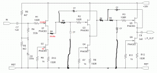
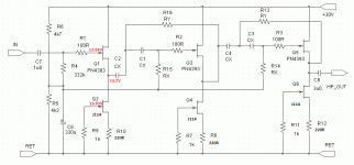
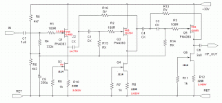
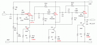
Attached schematics HP & LP with measurements.
Attachments
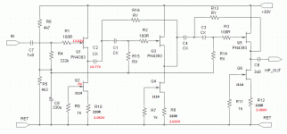
for this High Pass Filter, the input Buffer has a -0.95Vgs
You should be able to measure the Vgs of the next two Filter Buffers and for similar devices you should get similar Vgs.
You also need to check your Low Pass Filter.
Each volt of Vgs add together by the end and significantly reduce the output voltage swing.
Since these are single ended amplifiers you don't want "normal" maximum signals to exceed around 50% of the absolute maximum output swing. Your 30V supply allows approximately +-14Vpk for a centred output offset. This allows a fairly clean 5Vac as the output.
If your output offset has moved up by 6V then the maximum swing is changed to ~14-6 = +8Vpk, -20Vpk. That equates to a fairly clean output of 3Vac.
You must check for this.
BTW,
you can reduce (or even eliminate) the output offset by adding the resistor as described in D.Joffe's paper on jFET Buffers.
For identical upper and lower jFETs, the added resistor matches the lower Rs, i.e. 220r in your diagram.
Last edited:
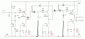
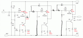
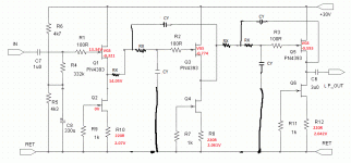
Attached pic with VGS measurements RED probe gate BLACK probe source. Measurement HP board I VGS Q3 shows a positive voltage
Please could you attach papers or link for D.Joffe's paper on jFET Buffers.
Please could you attach papers or link for D.Joffe's paper on jFET Buffers.
Attachments
- Status
- This old topic is closed. If you want to reopen this topic, contact a moderator using the "Report Post" button.
- Home
- Source & Line
- Analog Line Level
- JFET Active Crossover