Why Sonnya? We don't want a 7W resistor here, a 5W would be more than sufficient.
Imagine 3.5A peak, that's 2.47A rms, and with 0R15 dissipation is one half of 2.47 squared x 0.15 which is 0.46W. This is continuous, 50W into 8R, absolutely flat strap. So 5W is more than enough as I usually simply triple the worst case!
It's 25mm, should be close enough for government work......
Hugh
Last edited:
The bodylength of the Ohmite is 23.8/25.8mm and then you need a few mm in each en to bend the wires.
But again, this is if you would like to make space to the ohmite. There is plenty of room for the 3W 13FR150 in your layout at the present state.
Sorry for asking, it was not ment to question your layout. It surely looks good.
It is only to be sure, as i make the same mistake once in a while
But again, this is if you would like to make space to the ohmite. There is plenty of room for the 3W 13FR150 in your layout at the present state.
Sorry for asking, it was not ment to question your layout. It surely looks good.
It is only to be sure, as i make the same mistake once in a while
Hey, Sonnya, give me tips by all means.
I'm leery of using resistors that are unnecessarily big. In truth a 3W source resistor is quite adequate. There is space there for 5W sandcast as well.
You are right about mistakes; I made my last in 1967, quite a serious one.....
Steve,
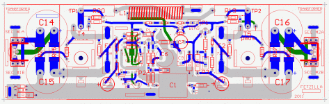
INSIDE the inductor, which accounts for the additional hole left and right at the centerline. It's a very compact way of doing it.
I think we have all bases covered now for the output stage fb take off point, thanks for bringing it up. I wasn't happy with the original either.
Cheers,
Hugh
I'm leery of using resistors that are unnecessarily big. In truth a 3W source resistor is quite adequate. There is space there for 5W sandcast as well.
You are right about mistakes; I made my last in 1967, quite a serious one.....
Steve,
INSIDE the inductor, which accounts for the additional hole left and right at the centerline. It's a very compact way of doing it.
I think we have all bases covered now for the output stage fb take off point, thanks for bringing it up. I wasn't happy with the original either.
Cheers,
Hugh
D.Self disagrees........ what is important is that the feedback is taken from the midpoint.
I disagree, many disagree.
The NFB tapping point must come off the output trace. It must not be taken off the Re connecting trace.
Midpoint has nothing to do with correct NFB tapping point.
Feeback should be taken after the summing point of both outputs. Whether or not the summing point is centered cannot matter any more then the Vbe diferences and emitter resistor variances, as long as the traces are large enough to carry their loads gracefully. Unless perhaps if EMI is a concern, but probably not?
If the both the output node and NFB are taken at the summing junction, small errors in the junction geometry will cause distortion. However much it matters is anyone's guess, but good practice is good practice. Especially when it holds back a frenzy of correction posts.
- keantoken
If the both the output node and NFB are taken at the summing junction, small errors in the junction geometry will cause distortion. However much it matters is anyone's guess, but good practice is good practice. Especially when it holds back a frenzy of correction posts.
- keantoken
D.Self disagrees.
I disagree, many disagree.
The NFB tapping point must come off the output trace. It must not be taken off the Re connecting trace.
Midpoint has nothing to do with correct NFB tapping point.
Well, it is taken from the centerpoint or should we say starpoint. And as long it is taken from the startpoint where the two resistors meets with the outputcoil it is perfectly ok. I do not expect any degration because of that.
Secondly Hugh has build many wellsounding amps according to the audience so he knows what he is doing.
I also have the textbook. We are talking 10mm offset, in dself book... That is right. then i agree but in the latest layout Hugh has made we are talking 1 - 2mm offset if not less. But you can try calculate the sq.area of both sides of the junction/ summingpoint
A much bigger issue where the ground potential is taken for the Feedback loop. You have much less signal/noise ratio here than at the output.
A much bigger issue where the ground potential is taken for the Feedback loop. You have much less signal/noise ratio here than at the output.
Andrew, any further suggestions? Your earlier one was correct, and I have made the changes, I believe this hits the spot. How did your tests go with and without lag compensation?
I have done a dissipation study of the semis. With an output stage bias of 500mA, VAS current of 12mA and 36V rails, T1 dissipates 77mW, T2 dissipates 420mW, T3 is 120mW and each of the output devices is 18 watts. The heatsink load is thus 36W, and with a Conrad 300x75 0.42C/W sink the rise above ambient is calculated to around 15C assuming all heat passes to the heatsink. On a day of 40C, a 60C heatsink with the amp operating at moderate output is just acceptable, so it should be OK. At all other temperatures, things look peachy.
Cheers,
Hugh
Attachments
Last edited:
I reported last night that I was listening without the miller comp cap.
I have not tried switching it in and out for comparisons yet.
Without M. comp and FM as source it still sounds nice.
I have supply rails +-28.5Vdc to +-29.5Vdc, so -20dB ref max power is ~2.5Vpk or ~2Vac I am still listening still without volume control and without pre-amp.
BTW the amp perforated board is 1.5" by 2.1" (3.5sqinches). That's 2 pairs of stereo boards from 100sq cm of PCB. Adopting smd could allow a few facilities on the same size PCB. Maybe soft start input mute and unmute, DC detect and signal out to relays/FET switches, DC servo.
It really does need a soft input mute for turning off.
Last edited:
")
I don't have any upstanding resistors. All are laid flat, 600mW, 1%, 50ppm, metal film.
I seem to remember Holco recommended the leads of their high precision resistors must be radiused after they exit the body and not "bent" at right angles nor bent near the body. This recommendation suits usptanding resistors and if the PCB is vertical it also ensures that all resistors are horizontal and thus more evenly heated to take advantage of the precision.
I seem to remember Holco recommended the leads of their high precision resistors must be radiused after they exit the body and not "bent" at right angles nor bent near the body. This recommendation suits usptanding resistors and if the PCB is vertical it also ensures that all resistors are horizontal and thus more evenly heated to take advantage of the precision.
Last edited:
Andrew,
It is self defeating to make this amp too small if you are dissipating quite high power from the output devices, which therefore should be reasonably far apart for best heat distribution.
Soft mute may be desirable, but it is not essential. In practice I'm sure the slight thump at turn-on is of little concern. DC sense could easily be accommodated on a separate board, with a suitable relay - go for it!
The idea is to keep it simple, and easy to build and get going.
Hugh
It does not thump at turn on. It appears to play music instantly.Soft mute may be desirable, but it is not essential. In practice I'm sure the slight thump at turn-on is of little concern.
The bigger problem is turn off.
My one plays normally for about 10seconds and by then the rails are so low the tiny signal I am passing to the speakers becomes more and more clipped for about a further minute as the discharge slows down to a crawl.
A FET input mute that brings the signal to ON and then turns it to OFF as a fade would be ideal.
at the moment I am at +-29Vdc and 300mA quiescent current. That's a total of 17.4W. I am using a 15mm thick backplate on a 0.6C/W sink. The devices are direct coupled to the sink (no Source resistors) and yet it runs @ ~ blood heat. There is no problem. My devices are @ the corners of the 1.5" wide dimension, i.e. 5 empty 0.1" pin pitches apart.It is self defeating to make this amp too small if you are dissipating quite high power from the output devices, which therefore should be reasonably far apart for best heat distribution.
If I were designing for Ta<=40degC rather than <=30degC, then I might increase the distance between the PCB and the sink, but I would not consider making the PCB bigger. The gate stoppers become the links between the PCB and the outputs.
Last edited:
- Status
- This old topic is closed. If you want to reopen this topic, contact a moderator using the "Report Post" button.
- Home
- More Vendors...
- AKSA
- Swordfishy/ASPEN FETZILLA power amp