Just found, maybe of interest:
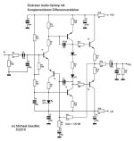
Vorverstärker mit diskretem OpAmp und komplementärer Differenz-Eingangsstufe
Vorverstärker mit diskretem OpAmp und komplementärer Differenz-Eingangsstufe
Attachments
A short note
I copied the orthography of the headline blindly and somewhat carelessly from the source, i.e. Burkhard Kainka's website. He will not have noticed the spelling mistake until today.
It certainly does not mean complimentary, in the sense of free of charge, but the term complementary!
Sorry for that quick mistake - that's pretty embarrassing.
Attachments

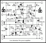
What can you expect from this simple circuit?
Certainly not the low distortion that can be achieved with the latest super OpAmps. But the results - as the spectrogram above shows - are certainly impressive. The total THD distortion of 0.004 percent is only slightly higher than the distortion products of the test generator (measured with a 24-bit sound card at a sample rate of 48,000 Hz). The signal was set to -6 dB(FS) at full scale of the card (approx. 1 volt) and 1000 Hz. At 0.0031 percent, the "good-natured" 2nd order distortion predominated; the disharmonic 3rd order distortion only reached 0.0021 percent, all higher distortion products were even lower. That's something to be proud of!
I don't yet recognize the big clou of this circuit form, I still have to think about it. But maybe it will solve one or two problems in a very tricky way ...

Oh yes,You can also add emitter degeneration to a complementary differential pair. You don't get cancellation of even-order distortion, like in a balanced ordinary differential pair.
that's right,
I only realized that at second glance.
Michael Gaetke wrote:
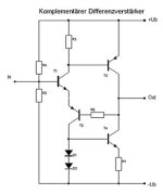
As you can easily see, T4, the diodes D1 and D2 and the resistor R1 form a constant current source. The current through T4 also defines the collector current of T3. As this current is constant, a constant voltage is also set at the base of T3 and the current through R3 and thus through the complementary differential input stage is also kept constant. This current is also the operating current of the reference diodes for the current source. The ring of four transistors T1 to T4 thus ensures its own quiescent current balancing. (...)
One advantage of the complementary arrangement is that the quiescent current of the differential input stage is not limited by a current source. Due to this limitation, the conventional input stage is sometimes unable to supply the current required to recharge the internal capacitors at the output quickly enough with certain pulsed input signals. In this case, the slew rate is limited, resulting in transient distortion.
Does this mean that this circuit form is now automatically TIM-free?
BTW,
thx Hugo
") .
.You mean is it free of slew-rate limiting? No, because you can't drive the current below zero so it can slew limit in one direction - the load capacitance can't be discharged beyond a certain rate, so it has a slew-rate limit but only in one direction. I suspect its stability can also be affected if driven to the point of current-starvation in the pair too.
- Home
- Source & Line
- Analog Line Level
- new - old design (Complementary Long Tailed Pair -> Complementary Difference Amplifier)