This is a differential ECL. One tap(T1 and T13) is the current switch(T1) and current source(T13). If you remove T13 and connect the collector and the emitter, you have typical ECL buffer with a differential input. I'm sure active current source is better than passive one constructed by one register, though I need to do some trial and error with the real PCB.
T1 is non-saturated current switch driven by SSTL15. In 1 state, LP_0 is 0.75+0.35=1.1V, LN_0 is 0.75-0.35=0.4V. In 0 state, LP_0 is 0.75-0.35=0.4V, LN_0 is 0.75+0.35=1.1V. The difference(0.7V) is enough to turn on or off the two transistors of T1. The transition time is minimal (0.2nS) because SSTL15 is up to 800MHz capacity. The disadvantage of ECL is the difference between turn on and off. Turn on is active while turn off is passive. I don't know how much it dominates the performance. But you are almost free from disturbance caused by digital switching, though terminated transfer(75 ohms), small voltage swing(0.7V) and non-saturation(constant current) are in favor for you.
FPGA(xc6slx9 in QFT144) has 25 differential SSTL15 drivers with the internal 75-ohm resistor. That's why you need two FPGAs for stereo DAC(I need 24 drivers for one channel). But two chips have the advantages, where PCB layout is easier than one large FPGA, and DIY friendly package(QFP) is available. One FPGA for one channel isn't a bad design.
As to JFET, I know high-speed analog switches supplied by AD and have some experience with them before. They are not discrete part but monolithic one for me, which means fine adjustment isn't available. I have no experience with a single JFET for high-speed switching. It's easy for me to use a transistor for "pulse" to analog conversion with FPGA which have the job in the digital domain, i.e., PCM to DSD conversion, pulse width adjustment for compensating the difference between turn on and off and optimum usage of 24 taps.
Would it be better to run your dif pair collector OP 'rails' into virtual ground
configured opamps?
Ye's I know this will require a further summing opamp.
T
I've thought a bit more about JohnW's remark about crosstalk from the flip-flops to the RTZ logic gates. One of the reasons why I have LC-filters between the regulator that supplies the flip-flops and the RTZ logic gates is to reduce this crosstalk. Separate regulators would probably be better. In either case, it would indeed be nice to time the flip-flop activity such that the impact of this crosstalk is minimized.
The flip-flops that clock in the raw input data will draw data-dependent current pulses that depend on both the new and the old bits. The filtering effect of the supply (inductive voltage regulator with capacitive decoupling and some damping term) will smear out these pulses in time. Hence, when the same regulator supplies the RTZ logic (or the resynchronization flip-flops, if those are used as the DAC), it is not possible to time the flip-flop activity such that it doesn't disturb the RTZ logic at all.
Nonetheless, the crosstalk path will often behave more or less as a differentiator to time or as a high-pass filter with a very small time constant. Examples are common impedance crosstalk across the parasitic inductance of a decoupling capacitor or crosstalk via a mutual inductance between current loops.
With a differentiating crosstalk path, there will be hardly any low-frequency crosstalk, but high-frequency crosstalk that gets multiplied with the datastream could still produce low-frequency components (at the difference frequencies between crosstalk and datastream). Hence, in these cases, it should help to only allow the data flip-flop to switch during the blanking period (no matter whether the blanking level is the same as the 0 level or somewhere halfway between the 0 and 1 levels - just as long as it's the same for each clock period, so no downmixing of high-frequency interference can occur).
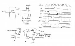
A normal master-slave type D-flip-flop consists of two latches, an input latch and an output latch. After a falling edge, the input latch becomes transparant and starts following the input data. After a rising edge, the input latch is locked and the output latch becomes transparent and takes over the data from the input latch. Hence, ideally both the falling and the rising clock edge of the input flip-flop should occur during the blanking period with some margin on either side to allow for RTZ logic delay. The clock should be high when the actual data are output from the RTZ logic. (For a flip-flop with clock enable, usually implemented as an input multiplexer, the clock may switch, but the clock enable should only be high during the blanking interval, with some margin on either side.)
Making a FIRDAC with cells that work on opposite clock edges becomes impossible, because otherwise there are no time intervals left when the data flip-flops are allowed to be active. Hence, the circuit will become sensitive to duty cycle and using a clock at a multiple of the bitrate and a clock divider to get a very well-defined duty cycle becomes necessary.
With a clock divider, to avoid accumulation of jitter, it starts to make sense to have resynchronizing flip-flops on the outputs. As these process only RTZ data, they are allowed to switch outside of the blanking interval. In fact they have to, to get any signal out at all.
All in all, I then end up with the attached circuit. The blanking interval has to be at least three and preferably four input clock cycles, so if you don't want to lose more than 50 % of the signal, you need at least six to eight clock cycles per bit period.
Note that only the output flip-flops should be supplied by the reference supply, as this ensures a pattern-independent load on the reference, because in each bit period, there is precisely one of these flip-flops producing an output pulse. Depending on the data, it is either the flip-flop connected to OUTM or the flip-flop connected to OUTP. This also means that these flip-flops should match, so a dual flip-flop is more favourable than two separate ones.
For my DAC all of this would not have been very useful, as there is always activity from the FIR filters in the FPGA outside the blanking interval. That is, I need to rely on the isolation between different supplies anyway. I did choose the FPGA clock frequencies such that at least FPGA clock harmonics that somehow leak into the DAC reference produce no whistles.
The flip-flops that clock in the raw input data will draw data-dependent current pulses that depend on both the new and the old bits. The filtering effect of the supply (inductive voltage regulator with capacitive decoupling and some damping term) will smear out these pulses in time. Hence, when the same regulator supplies the RTZ logic (or the resynchronization flip-flops, if those are used as the DAC), it is not possible to time the flip-flop activity such that it doesn't disturb the RTZ logic at all.
Nonetheless, the crosstalk path will often behave more or less as a differentiator to time or as a high-pass filter with a very small time constant. Examples are common impedance crosstalk across the parasitic inductance of a decoupling capacitor or crosstalk via a mutual inductance between current loops.
With a differentiating crosstalk path, there will be hardly any low-frequency crosstalk, but high-frequency crosstalk that gets multiplied with the datastream could still produce low-frequency components (at the difference frequencies between crosstalk and datastream). Hence, in these cases, it should help to only allow the data flip-flop to switch during the blanking period (no matter whether the blanking level is the same as the 0 level or somewhere halfway between the 0 and 1 levels - just as long as it's the same for each clock period, so no downmixing of high-frequency interference can occur).
A normal master-slave type D-flip-flop consists of two latches, an input latch and an output latch. After a falling edge, the input latch becomes transparant and starts following the input data. After a rising edge, the input latch is locked and the output latch becomes transparent and takes over the data from the input latch. Hence, ideally both the falling and the rising clock edge of the input flip-flop should occur during the blanking period with some margin on either side to allow for RTZ logic delay. The clock should be high when the actual data are output from the RTZ logic. (For a flip-flop with clock enable, usually implemented as an input multiplexer, the clock may switch, but the clock enable should only be high during the blanking interval, with some margin on either side.)
Making a FIRDAC with cells that work on opposite clock edges becomes impossible, because otherwise there are no time intervals left when the data flip-flops are allowed to be active. Hence, the circuit will become sensitive to duty cycle and using a clock at a multiple of the bitrate and a clock divider to get a very well-defined duty cycle becomes necessary.
With a clock divider, to avoid accumulation of jitter, it starts to make sense to have resynchronizing flip-flops on the outputs. As these process only RTZ data, they are allowed to switch outside of the blanking interval. In fact they have to, to get any signal out at all.
All in all, I then end up with the attached circuit. The blanking interval has to be at least three and preferably four input clock cycles, so if you don't want to lose more than 50 % of the signal, you need at least six to eight clock cycles per bit period.
Note that only the output flip-flops should be supplied by the reference supply, as this ensures a pattern-independent load on the reference, because in each bit period, there is precisely one of these flip-flops producing an output pulse. Depending on the data, it is either the flip-flop connected to OUTM or the flip-flop connected to OUTP. This also means that these flip-flops should match, so a dual flip-flop is more favourable than two separate ones.
For my DAC all of this would not have been very useful, as there is always activity from the FIR filters in the FPGA outside the blanking interval. That is, I need to rely on the isolation between different supplies anyway. I did choose the FPGA clock frequencies such that at least FPGA clock harmonics that somehow leak into the DAC reference produce no whistles.
Attachments
Wow, interesting. I always used them for sine to square conversion on my
clocks.
It's a pity he didn't get to measure Potato Logic in direct comparison.
I've thought a bit more about JohnW's remark about crosstalk from the flip-flops to the RTZ logic gates. One of the reasons why I have LC-filters between the regulator that supplies the flip-flops and the RTZ logic gates is to reduce this crosstalk. Separate regulators would probably be better. In either case, it would indeed be nice to time the flip-flop activity such that the impact of this crosstalk is minimized.
The flip-flops that clock in the raw input data will draw data-dependent current pulses that depend on both the new and the old bits. The filtering effect of the supply (inductive voltage regulator with capacitive decoupling and some damping term) will smear out these pulses in time. Hence, when the same regulator supplies the RTZ logic (or the resynchronization flip-flops, if those are used as the DAC), it is not possible to time the flip-flop activity such that it doesn't disturb the RTZ logic at all.
Nonetheless, the crosstalk path will often behave more or less as a differentiator to time or as a high-pass filter with a very small time constant. Examples are common impedance crosstalk across the parasitic inductance of a decoupling capacitor or crosstalk via a mutual inductance between current loops.
With a differentiating crosstalk path, there will be hardly any low-frequency crosstalk, but high-frequency crosstalk that gets multiplied with the datastream could still produce low-frequency components (at the difference frequencies between crosstalk and datastream). Hence, in these cases, it should help to only allow the data flip-flop to switch during the blanking period (no matter whether the blanking level is the same as the 0 level or somewhere halfway between the 0 and 1 levels - just as long as it's the same for each clock period, so no downmixing of high-frequency interference can occur).
A normal master-slave type D-flip-flop consists of two latches, an input latch and an output latch. After a falling edge, the input latch becomes transparant and starts following the input data. After a rising edge, the input latch is locked and the output latch becomes transparent and takes over the data from the input latch. Hence, ideally both the falling and the rising clock edge of the input flip-flop should occur during the blanking period with some margin on either side to allow for RTZ logic delay. The clock should be high when the actual data are output from the RTZ logic. (For a flip-flop with clock enable, usually implemented as an input multiplexer, the clock may switch, but the clock enable should only be high during the blanking interval, with some margin on either side.)
Making a FIRDAC with cells that work on opposite clock edges becomes impossible, because otherwise there are no time intervals left when the data flip-flops are allowed to be active. Hence, the circuit will become sensitive to duty cycle and using a clock at a multiple of the bitrate and a clock divider to get a very well-defined duty cycle becomes necessary.
With a clock divider, to avoid accumulation of jitter, it starts to make sense to have resynchronizing flip-flops on the outputs. As these process only RTZ data, they are allowed to switch outside of the blanking interval. In fact they have to, to get any signal out at all.
All in all, I then end up with the attached circuit. The blanking interval has to be at least three and preferably four input clock cycles, so if you don't want to lose more than 50 % of the signal, you need at least six to eight clock cycles per bit period.
Note that only the output flip-flops should be supplied by the reference supply, as this ensures a pattern-independent load on the reference, because in each bit period, there is precisely one of these flip-flops producing an output pulse. Depending on the data, it is either the flip-flop connected to OUTM or the flip-flop connected to OUTP. This also means that these flip-flops should match, so a dual flip-flop is more favourable than two separate ones.
For my DAC all of this would not have been very useful, as there is always activity from the FIR filters in the FPGA outside the blanking interval. That is, I need to rely on the isolation between different supplies anyway. I did choose the FPGA clock frequencies such that at least FPGA clock harmonics that somehow leak into the DAC reference produce no whistles.
I still have difficulties wrapping my head around this, but delaying and dividing clocks can be done with this device:
LTC6954 Datasheet and Product Info | Analog Devices
It's easy to program with a Linduino (slightly modified arduino, though it can be used as well with a small adaptation). Its got excellent jitter specs, can delay multiple clockcycles and divide in integer steps to 63 and options of various output types (cmos pecl etc).
In general it could be the heart of a versatile and high quality clocking core, which might come in handy when you don't have the capability to go for fpga's etc;-)
Another good divider/delay with a slightly different feature set: http://www.ti.com/product/LMK01000
Wow, interesting. I always used them for sine to square conversion on my
clocks.
It's a pity he didn't get to measure Potato Logic in direct comparison.
Has anyone actually measured the Potato stuff? I find their whole website and distribution model to be sketchy to say the least. Demian did post a while ago that they were legit, but I don't recall if that was personal experience or word-of-mouth.
@xx3stksm: Just a brief comment to your #2217 post - which I'm also not entirely sure is relevant - but anyway here it is:
Arto Kolinummi in his book "Audio Power Amplifiers - towards inherently linear amplifiers" mentions some studies he made on transistors with various packages. He tested for thermal distortion i.e what happens to a transistor's characteristics when heated/cooled. And found that various packages stabilized, or the opposite, the characteristics of the transistor. Typically larger packages showed less distortion likely due to their greater heat capacity (e.g. SOIC-8 vs SOT-23),
I am mentioning this because I notice that you are considering using very small transistors in your DAC design - might some kind of thermal dynamic distortion be introduced by this?
@Marcel & more: I have something else to attend to these days so I can't fully give attention to the RTZ discussion. Yet it sounds indeed interesting so I hope to follow it on and off as time allows ...
Cheers,
Jesper
I'd like to just quickly mention that I see many designs where only a single filter capacitor is strapped between the differential outputs of the LPF - this is EXTREMELY bad practice as this can ONLY filter the differential noise products - offering zero filtering to common mode noise signals. This single capacitor strapped between the Diff pairs should be replaced with two capacitors - one on each Diff output to Ground (the capacitors will need to be x2 in capacitance value of the original single capacitor to maintain the same filter response as they are in effect in series with each other).
I see this arrangement on so many manufacturers datasheets where they should really know better...
Hi, John,
Isn't the concern that utilizing two shunt capacitors to ground requires they be tightly matched, else the CMRR of the following difference amplifier stage largely degrades, and any common-mode noise imbalance gets converted to difference mode noise? Even capacitors matched to 1% only support around 40dB of CMRR. Doesn't an single differentially connected capacitor leave the full CMRR of the following difference amplifier stage intact, and inherently not convert any common-mode noise to difference mode?
Last edited:
Marcel, Could this rtz style 'no dac' be made into a simple project? Similar to others efforts in this thread? Make a run of boards for it? This can handle PCM and DoP? And Native DSS? If so I'll just wait and see where this goes.")
If you want to keep it simple, it will become a DSD-only DAC with a raw DSD interface. If there is a master clock available at an integer multiple of eight times the DSD rate, it can be the version of post 2223, otherwise the simple NOR-gate/AND-gate version.
Hi, John,
Isn't the concern that utilizing two shunt capacitors to ground requires they be tightly matched, else the CMRR of the following difference amplifier stage largely degrades, and any common-mode noise imbalance gets converted to difference mode noise? Even capacitors matched to 1% only support around 40dB of CMRR. Doesn't an single differentially connected capacitor leave the full CMRR of the following difference amplifier stage intact, and inherently not convert any common-mode noise to difference mode?
Yes, that's definitely a concern, and what Marcel recommended is a good idea. Also, you could use an X2Y capacitor which might ensure better matching of the caps.
Yes, that's definitely a concern, and what Marcel recommended is a good idea. Also, you could use an X2Y capacitor which might ensure better matching of the caps.
X2Y capacitors seems a good suggestion. I believe that I once saw a balance spec. for them where they enable up to 90dB of CMRR.
- Home
- Source & Line
- Digital Line Level
- The Best DAC is no DAC