tschrama said:
I just got this idea. It is the I/V stage for my latest DAC project...(4th allready.. I'm going to be a real DIY pro one day)
I didn't measure it.. ain't got no distortion or spectrum analyser, but how do you guys feel about this one? I simulates great....
Very nice Current to Voltage amplifier, tschrama
Simple & good.
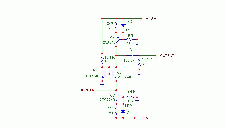
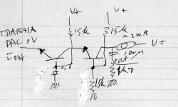
Schematic:
http://www.diyaudio.com/forums/attachment.php?postid=77793&stamp=1036433748
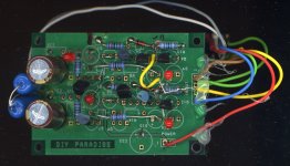
The original circuit built.
I wonder if tschrama's circuit was ever built?
Anyway. I am very glad I finally tried the original circuit from this thread. The number one post from Jocko Homo.
It's very interresting because it seems every one in this thread are sitting in their armchairs and bring comments. Only very few have tried to build the original circuit? It really works great and the music dynamic is huge!
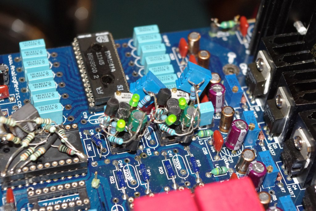
I use 270 ohm on R3 and R4. 10k pot on R4. R5 and R6 are 10k. R1 4.7k and C1 47uF. Green LED's. Transistors are BC546B and BC557B. It didn't work at all before I paralelled R3 with a pot on 1k ohm. I adjust it for least distortion (1khz test CD).The voltage on Q2 collector then settles on about 8.6 V.
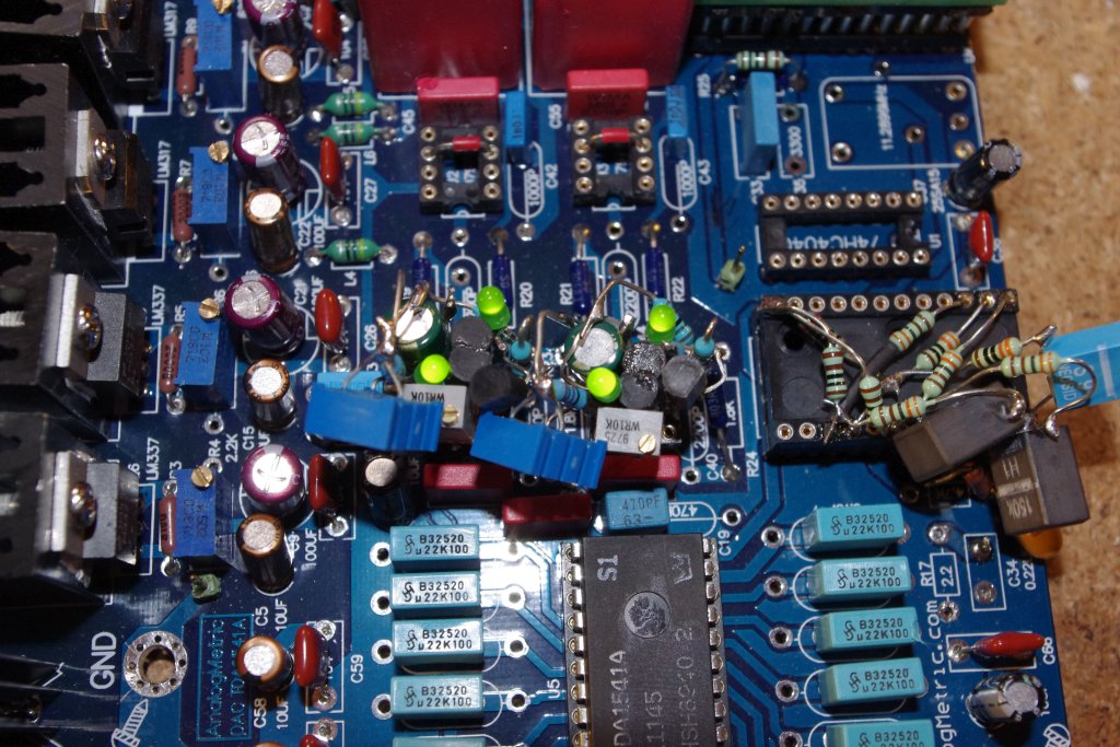
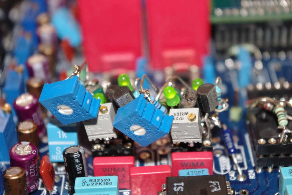
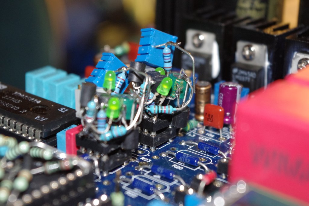
It's sensitive in adjusting the CCS but after it's done I am really impressed. Less is not always better but in this case I can't find anything negative. In the pictures below you can see my handcrafted prototype beauties
You can also see another mod. I2S attenuators. There is some talking about using these attenuators will give the TDA1541 only the needed zeroes and ones. It doesn't have to bounce between 0 and 5 volt and possible give artifacts on the sound trough overhearing in the substrate on the IC.
I wonder if tschrama's circuit was ever built?
Anyway. I am very glad I finally tried the original circuit from this thread. The number one post from Jocko Homo.
It's very interresting because it seems every one in this thread are sitting in their armchairs and bring comments. Only very few have tried to build the original circuit? It really works great and the music dynamic is huge!
I use 270 ohm on R3 and R4. 10k pot on R4. R5 and R6 are 10k. R1 4.7k and C1 47uF. Green LED's. Transistors are BC546B and BC557B. It didn't work at all before I paralelled R3 with a pot on 1k ohm. I adjust it for least distortion (1khz test CD).The voltage on Q2 collector then settles on about 8.6 V.
It's sensitive in adjusting the CCS but after it's done I am really impressed. Less is not always better but in this case I can't find anything negative. In the pictures below you can see my handcrafted prototype beauties
You can also see another mod. I2S attenuators. There is some talking about using these attenuators will give the TDA1541 only the needed zeroes and ones. It doesn't have to bounce between 0 and 5 volt and possible give artifacts on the sound trough overhearing in the substrate on the IC.
no real bass....
What!?
The bass is where this circuit shines the most. Really heavy, punchy, clean and low and revealing details. At least in my NOS DAC.
You must have done something wrong?
I tried soooo many circuits and transformers....
Also Pedja Rogic schemes with AD844 and OPA861. And a shoebox full of "opamps" including discrete opamps like my own, OPA-EARTH, OPA-SUN.
BTW R1 should be to the left side of C1.
And if you use the TDA1541 you need to cancel the offset current from the DAC with a CCS like Pedja did. Just a BF245.
Last edited:
Hi Patrick,> I tried soooo many circuits and transformers....
So what would you suggest as your most favorite solution ?
Transformers ?
Patrick
Yes I am finally very happy with Sowter transformers and AD1865N-K.
So it's kind of Audio Note DAC but not with tubes.
http://www.sowter.co.uk/dacs.php
Last edited:
Wrong! Gives 20db higher distortion regarding Jockos comments. Read the thread. You mean he was wrong on that? then I'll take it back and will test it as you say.BTW R1 should be to the left side of C1.
I don't understand. You mean that this simple circuit actually is that heavily flawed?And if you use the TDA1541 you need to cancel the offset current from the DAC with a CCS like Pedja did. Just a BF245.
It seems to me that your statement indicates you havent built and/or understood the circuit. I'm very sorry, but for the moment I have a stable 0.3mV at the DAC's outputs.
Can you show schematic on Pedja's circuit?
Cheers
 [
[
Last edited:
Hi aparatusonitus
If i have current offset wouldn't it show up as a voltage offset att output?
Is this somekind of an holy grail kept secret that never is to be mentioned? "The lost symbols of TDA1541A"
Or did you all people, with very short comments, had personal contact with Jocko Homo and won't dare to tell and explain how things work, because of Jockos dislaking of sharing schematics to people who knows how to solder and do PCB's ? This is somewhat amusing, even if it's a bit frustrating.
Cheers to all DIY people. It's late dinner time for me, with lost of red wine. Maybe I have some answers later on this evening.
If i have current offset wouldn't it show up as a voltage offset att output?
Is this somekind of an holy grail kept secret that never is to be mentioned? "The lost symbols of TDA1541A"
Or did you all people, with very short comments, had personal contact with Jocko Homo and won't dare to tell and explain how things work, because of Jockos dislaking of sharing schematics to people who knows how to solder and do PCB's ? This is somewhat amusing, even if it's a bit frustrating.
Cheers to all DIY people. It's late dinner time for me, with lost of red wine.
Maybe I have some answers later on this evening.1st it's is not Jocko's schematic, it's just a simplified idea he posted a while ago. Jocko's original circuit is way more complicated and I will not post it here or anywhere in respect of his IP.Hi aparatusonitus
If i have current offset wouldn't it show up as a voltage offset att output?
Is this somekind of an holy grail kept secret that never is to be mentioned? "The lost symbols of TDA1541A"
Or did you all people, with very short comments, had personal contact with Jocko Homo and won't dare to tell and explain how things work, because of Jockos dislaking of sharing schematics to people who knows how to solder and do PCB's ? This is somewhat amusing, even if it's a bit frustrating.
Cheers to all DIY people. It's late dinner time for me, with lost of red wine.
I have built the simple circuit on a diyparadise board obtained from Yeo. Sometimes it did not work as the voltage left of cap C1 is not defined as remarked in post # 12 of this thread. It did work when I added 10k there....
The good point of these common base circuits is it does not give digital glare. The bad I already mentioned no bass slam.
Without compensating TDA1541 current you have extra current into the IV, you can compensate for that with a JFET constant current source, or make the whole thing even single ended as in my picture.
Attachments
Last edited:
.... Jocko presented the simplified one as his own... didn't he? "My circuit will function" or some similar sentence he says in this very thread.1st it's is not Jocko's schematic, it's just a simplified idea he posted a while ago. Jocko's original circuit is way more complicated and I will not post it here or anywhere in respect of his IP.
I have to ask .. is IP some sort of patent? Anyway ... way more complictated I/V stage means to me no more discrete simple idea for this circuit. Then it's better to go integrated with some of the worlds best IC OP amps. .... but that offcource takes the feeling away, of using "the lost symbols of the holy grail sound approach"

Without compensating TDA1541 current you have extra current into the IV, you can compensate for that with a JFET constant current source, or make the whole thing even single ended as in my picture
That was not the informative documentation i hoped for, but I'm sure it was quick posted....
The lack of proper schematics and explenations in long texts as, for example the DIY member ECDESIGN's splendid posts, gives great opportunities for misinterpretations and misunderstandings all the way to the border where you feel dismissed and leave this forum.
I'm sorry but I don't think I need the current compensation you mention at all. Also the simplicity is way gone.
I will measure with my instruments this time, instead of just listening and I will put the OP's back again for compairing, just for the fun and the hell of the big free time I have to spend everyday (ironic joke)

At the age of 47 I have the skill, place, money and karma to do "things" but the time is the limit because of such matters as a family (which I also want to have and is a good thing) and work and other obligations, as cooking food for myself and others for example....

I envy Einstein who "worked" at the patent shop and did his own things when no one saw
Anyway, the things I find in my research ..for the moment the only empirical open research on this matter .. I will document on my homepage later on.
Stay tuned. I will try to be as openminded and give as much documentation as I have the time and skill to do ..
The grumpy old man is now going to bed .. or take a listenings session to my "non working" I/V stage. (Ironical and sarcastic as allways)


FFT on this very first post schematic
I have gone a bit further in my learnings and joys of modding this splendid DAC. Lots of sparetime trough this weekends and burning desire is the recepie.
I now have a near complete homepage on this project which now gives rather good information I believe. I hope it can bring some more idés up.
To the point. In this homepage I now have totally subjective thoughts about the circuit from the first post of this thread.
Anyway, the non subjektive part is the two FFT graphs of the unit working at both -0dB and -60dB. Be my guest.
Last edited:
Did this ever work for ANYONE?!!!!
I tried to build this I/V over 10 years ago, and never got it to work, even after three build attempts.
There is a long discussion over on diyhifi.org detailing my various attempts. Seems other had issues, too.
I did get Rudolf B's similar (but simpler) I/V to work.
Anyone have success with Jocko's original ckt (per as per the OP schematic)?
I have had several requests for my I/V board. SInce they are now all gone, here is something you guys can throw together to hold you over until I build some new ones. It is close (distortion is -70 dB vs. -80 dB; input Z is 5 ohms vs. 0.1 ohms).
Hey, you really didn't think I was going to give you the good one for free did you? [joke]
You may need to tweak the current slightly of either CCS to get the collector of Q2 to a decent voltage. And also R4 to get the emitter of Q2 at exactly 0.0 V. (You guys need something left to try by yourselves.....I'm not going to do it all for you.) [joke]
Jocko
I tried to build this I/V over 10 years ago, and never got it to work, even after three build attempts.
There is a long discussion over on diyhifi.org detailing my various attempts. Seems other had issues, too.
I did get Rudolf B's similar (but simpler) I/V to work.
Anyone have success with Jocko's original ckt (per as per the OP schematic)?
Forgot to add ...
I only have 15v to work with, not the suggested 18v. Could the orig. be that sensitive to few volts less? Is it the fact that JH usedToshiba trans. (not common "BC")?
Connected/built (as per the original JH schema), all the LEDs light up, and I can hear a very faint (but distorted) music signal.
Not sure why Rudolf felt the need to modify the JH I/V (a few weeks later, back in 2002, after JH posted his "original")? There were folks that reported the JH ckt. did not work.
Hi,
QSerra gave a hint in #185 ..... saying that the common collectors of Q2and Q4 needed a dc path to a defined potential (a supply lin, gnd, etc).
As both collectors are high impedance it his highly improbable that a certain stable idle potential develops, but rather that the voltage is driven 'into' one of the collectors .... to a,most 0V or V+.
One could either omit with the current source Q4 and just use a load resistor connected from Q2s collector to V+, or use a current mirror mirrors into a gnd (or V-) referenced load resistor.
jauu
Calvin
- Status
- This old topic is closed. If you want to reopen this topic, contact a moderator using the "Report Post" button.
- Home
- Source & Line
- Digital Source
- Easy-to-build I/V stage