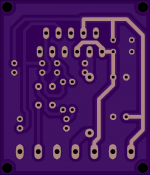
It would be fairly easy to guess the value from the layout. But a picture of the bottom layer would help a lot.
Thanks for your kind reply, I have attached also bottom layer please check.
Attachments
R7 is incomplete. It should be a power resistor in parallel with an Output Inductor.
I don't fit these two components on a cramped PCB. I believe it is better to mount the output inductor off the PCB and try to locate it in the cable running to the speaker terminal and away from chassis panels and away from the amp PCB, an extra inch or two of space is enough.
That inductor is air-cored. Wind 1mm to 1.6mm diameter enamelled copped wire around an AA battery. About 8 to 10turns is sufficient. You'll need about 400mm to 500mm to wind this.
Now that R7 is OFF board you need to add a wire to connect the chipamp's output terminal to the PCB screwed OUT terminal. A 1mm to 1.2mm diameter enamelled copper wire soldered direct to the chipamp's Pin3 (on the top side and that flat section before it turns down into the solder pad)
Last edited:
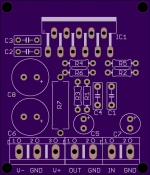
C1: input cap. Hard to fit bigger than 220nF from the footprint.
C3/C2: local hf decoupling. Looks like it's setup for something like 100nf/63V mkt from the footprint.
C4: appears to be the zobel cap. See this page for a table of values.
C5: feedback cap. Something like 100uF/10V
C6/C8 : local bulk decoupling. Use the biggest caps that fit, considering the required working voltage.
C7: mute cap, see the datasheet to calculate its value.
R1: RB in the datasheet, 1K
R2: sets the input impedance, 47k to 100k
R3: feedback resistor, 1k
R4: feedback resistor, 22k
R5: mute resistor, see c7
R6: zobel resistor, see C4
R7: output resistor, 10R/1W at least. See what Andrew said about it.
It's a fairly suboptimal layout missing the not so optional stability parts btw.
I wouldn't have taken speaker ground to/from the pcb.
It is normal to take it from main smoothing caps.
On a properly designed pcb, that would be suboptimal. See this article
On this one, I doubt either way would matter.
On a properly designed pcb, that would be suboptimal. See this article
On this one, I doubt either way would matter.
If you take speaker return to pcb the speaker return signal will modulate the ground.
I haven't seen an amp design yet where they didn't say return speaker to main smoothing caps.
Nigel won't listen.On a properly designed pcb, that would be suboptimal. See this article
On this one, I doubt either way would matter.
Better to modulate the ground with the signal than to modulate the feedback with the charging current. In a perfect world you would want to connect the feedback loop directly on the speaker terminals.
Better not to modulate anything !
The point directly between the smoothing caps is where the charge current is highest
But that's fine because that is the star ground point for high power.
The ground into the pcb takes milliamps so isn't important if the speaker return isn't taken to it as well.
I have done my time learning star grounding techniques.
I designed an audio mixer with no work on the grounds.
The output was 50Hz at 1 volt peak to peak with input grounded.
When I star grounded all the grounds instead there wasn't the slightest hint of 50Hz.
The power should always come in on one side and out on the other side of the smoothing capacitors. That way the charging impulses don't modulate the output ground.
The path between + on one smoothing capacitor center tap and the - on the other smoothing center tap should be as short as possible.
That's why my mixer didn't work, the charging impulses modulated the audio ground signal.
The path between + on one smoothing capacitor center tap and the - on the other smoothing center tap should be as short as possible.
That's why my mixer didn't work, the charging impulses modulated the audio ground signal.
- Status
- This old topic is closed. If you want to reopen this topic, contact a moderator using the "Report Post" button.
- Home
- Amplifiers
- Chip Amps
- Please help me with LM3886 PCB