The circuit of the DLH Super Buffer has been rearranged, in order to obtain a much wider adjustment with the trimpot that governs the symmetry of the output.
This allows to more easily explore several distortion profiles, which is the great potential of this buffer.
PowerPoint has been used to more easily visualize possible changes in the distortion profile.
These modifications can also be implemented in any of the versions of his older brothers, the DLH amplifiers.
I hope you enjoy it.
Attachments
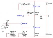
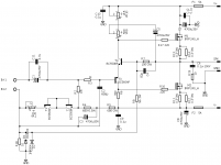
The new circuit of the DLH Super Buffer is in the Powerpoint file. For those who can not open it, here is the new schematic.
As you can see, the resistance of 390 ohms has been eliminated by the strategic relocation of the trimpot for the adjustment of bias. The number of components and the possibility of faults are reduced.

As you can see, the resistance of 390 ohms has been eliminated by the strategic relocation of the trimpot for the adjustment of bias. The number of components and the possibility of faults are reduced.
Attachments
Member
Joined 2009
Paid Member
This very simple design has all the ingredients to satisfy even the most demanding DIYers.
Great project.
")
Many thanks Nelson!!!. I have developed it from the beginning of simplicity, taking advantage of the potential of a differential amplifier in vertical disposition (very rare to see and in which its four terminals are used) and a stacked output.
The greatest of all my respects
The greatest of all my respects
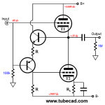
There were boards of earlier variants of this amp a few pages back. The new simplified one could probably be adapted from those boards. Although I haven’t seen any builds posted besides my own hand etched PCBs. This amp sounds very nice and can benefit from a muscular preamp like the Aksa Lender preamp that I am working on now. Also simple topology with very low distortion.
AKSA's Lender Preamp with 40Vpp Output
AKSA's Lender Preamp with 40Vpp Output
Member
Joined 2009
Paid Member
Attachments
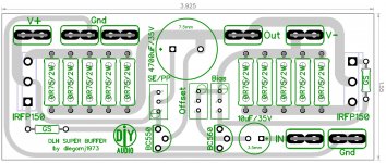
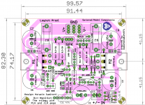
So I put together a pcb for the Super Buffer. If it looks ok I'll post the pdf's and the gerbers. The traces are 50 mil., I feel like they need to be fatter? Also, I didn't really like the placement of the V+/- spades. Suggestions are appreciated. Thanks.
Attachments
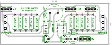
Very grateful for your effort, Ripcord. I really like the design and distribution of elements of your PCB. Possibly, it is necessary to increase the width of the tracks where the highest current circulates (+ V to Drain of upper mosfet, Source of upper mosfet to upper terminal of Rsource, Lower terminal of Rsource to Drain of lower mosfet, Source of lower mosfet to Upper terminal from Rsource; Lower terminal of Rsource a - V). This description is based on my schematic (not on your PCB).
For the rest, I like it very much .
.
For the rest, I like it very much
.
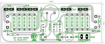
Ok thanks. Here are the changes you suggested. 100 mil traces on the higher current paths. I added some mounting holes and some heat vents under the 2W resistors.
The gate trace is quite long, on both mosFETs.
I think you should add a gate stopper into the two gate traces with the end of the resistor VERY close to the gate pin.
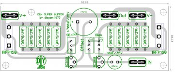
Compare to post39.
Last edited:
Very unique design Horacio,
May be not even imagined by the great designers of diya/ their commies all-over diya, whom people have a cult following. Wow...amazing thing .....
I am your fan....
Ripcord,
Nice pcb design. Like efortier says put something for the reference (gnd).
Regards
Prasi.
May be not even imagined by the great designers of diya/ their commies all-over diya, whom people have a cult following. Wow...amazing thing .....
I am your fan....
Ripcord,
Nice pcb design. Like efortier says put something for the reference (gnd).
Regards
Prasi.
Last edited:
Ok thanks. Here are the changes you suggested. 100 mil traces on the higher current paths. I added some mounting holes and some heat vents under the 2W resistors.
Nice layout Ripcord. It would be good to have the audio input going to four pads spaced for a combination of screw terminal blocks or 2.5mm pitch 2-pin JST PCB mount socket combo with one pin being ground. I appreciate you providing spade tabs for the other connections. I second AndrewT's suggestion of having a gate stopper very close to pin 1 of MOSFET. Perhaps 220R would be good. Not sure if needed but doesn't hurt.
Thanks,
X
A question for DiegoMJ, there was quite a bit of feedback capacitance used in previous circuit, have you found it unnecessary in practice?
Last edited:
Ok. Fixed missing trace, put in gate stoppers as per AndrewT, but for some reason was drawing a blank on the Gnd reference. I just put in a Gnd for the PSU, the output and the input and tied them together. Was that right? Also, I lost the mounting holes but I figured the TO-247 mounts would be strong enough to hold it to the heatsink.
P.S. I posted before I saw X's comment. I think I have that pattern so will add.
P.S. I posted before I saw X's comment. I think I have that pattern so will add.
Attachments
- Home
- Amplifiers
- Solid State
- DLH Amplifier: The trilogy with PLH and JLH amps