Hello all,
thanks to the help you guys are offering, i almost finished my project.
right now i`m in the dark again.
i`m using this box:
View attachment 583484
it allows me to get a coaxial and a spdif connection over usb.
it comes with it`s own asio windows driver and works very well.
i just realized i dont have a WS, DATA/L DATA/R only a BCK
i asume i need a different usb conversion board
can someone please recommend a suitable board.
many thanks
Hi xedox,
I would suggest looking into getting some of Iancanadas gear.
I am using 3 of his boards:
- SPDIF to I2S
- FIFO
- I2S to PCM
You could also looking at getting one of his clock PCBs if you dont already have one.
Its well worth the effort of using the PCM protocol to stream data into the 1541 simultaneously. The resulting "digital noise" inside the 1541 chip is reduced to about 25% when using 16bit/44.1k compared with using direct I2S in Time multiplexed mode. And when attenuated this noise is further reduced. My PCB is definitely optimised for the Simultaneous PCM protocol.
There are other products avaliable which I have no experience with:
-Audial - USB TO SIMULTANEOUS DATA (OR I2S) BOARD
-SdTrans384 (SD card reader with PCM output)
Ryan
Hi,
just want to say thanx to all members who helped me out.
@rayan, i was stupid enough not to think about this issues before starting the project.
i had a look at Ian`s huge project, i thought maybe get one of his I2S to PCM converter board and hook it up with the box i already have that gives me I2S.
i`m not sure if that is going to work though.
otherwise i`m going to run yor board in I2S mode for now, even if it means that i have to change the parts DR1-DR4
thanks
Xedox,
Notice you will need too feed the I2S PCM board from Ian via its inputt MCLK input uf-l plug with the output of an external Masterclock, for instance :
- the MCLK outputt of the Wave I/O (which has an uf-l outputt plug)... or
- the MCLK outputt of the Ian's Clock II board (which has an uf-l outputt plug as well)... or, always to stay in simultaneous (=PCM) mod :
Te Pedja's brand new USB to PCM board which need anything from a Masterclock as the Masterclock is embeded Inside (this is a standalone board so no need on a "long" 10" uf-l wire ! The price will be less expensive as all is integrated with only one shipping ! I never listened this one, but I'm sure Pedja Rogic makes good stuffs, as everyone as already pointed out here and everywhere. https://www.audialonline.com/topics/usb-to-simultaneous-data-or-i2s-board/ (many of us uses the AYA II for the TDA 1541A chip)
On a technichal side, the Ian's Canada solution has for it to have a FIFO which synchronise the three I2S signal to avoid the jitter issues. But is more expensive to integrate (although no sounding benchmark exists as the Pedja's board is being to be launched)
Having the same inputt config from bRyan but the isolator in plus, I can testimonie than it's sound good, with my Wave I/O board (which is the USB to I2S board). I find the Clock II from Ian with the CHD-957 crystals is not sounding harsch in my setup and with the AYA II. So you can go without fear for all the Ian's stuff as well ! Links already given before by a member just before.
I also tried only the Wave I/O (USB to I2S board) with the Ian's PCM board only and it sounds very good as well and even without the isolated (chip solution) outputt because I rather use the uf-l plugs outputts of the board which are not isolated (but the NDK crystals and board and great after sell support of Lucian Wave I/O Creator Worth it imho).
So now all is about your money and choice, but I personnally will advise to use only u-fl wires in your choice when it comes to plug two boards together in the DAC area.
Hope that technicaly helps,
Eldam
Hi Eldam,
many thanks for your detailed infos.
i`m left with 4 options now
1. i keep my USB to I2S box and run ryan`s board in I2S mode
2. i buy the necessary boards from Ian and run ryan`s board in simultaneous mode
3. i buy Pedja`s board USB to PCM and run ryan`s board in simultaneous mode
4. if you take a look at the picture in post 331 i have a MCK (masterclock) connector on my board. This makes me think that i could connect Ian`s I2S to PCM board to my box.
if i want simultaneous mode its probably wiser to buy Pedja`s board.
what bothers me is that the whole thing gets rather complicated
Pedja`s board needs external power supply, then another supply for ryan`s board.
i wanted to keep everything simple.
my existing board powers off usb directly, no external psu.
is it worth spending another 150 euros on Pedja`s board or even more on Ian`s gear to run simultaneous mode????
i own a arcam cd Player with a TDA 1541A double crown, this player sounds fantastic.
i think i am going to try rayan`s board with my usb to i2s board first. I will compare it to my arcam as well.
if i`am not pleased by the result i`ll probably buy Pedja`s board.
thank you
Last edited:
Yeah I would try it without first it will become pretty obvious if you have a stability issue or not (very low current draw very low voltages). One other thing I forgot to mention if using I2S mode you may want to consider not attenuating bck at all. Your mileage May Vary but I could never get it to sound right with the resistive attenuator.

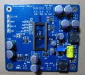
View attachment 585512
i decided on something like this
if i wont be satisfied im gonna power the board with rechargeable cells
Hi xedox,
It would be interesting to do a comparison between the board you posted and batteries anyway.
As i've mentioned before, im using batteries to power the 26V, 8V inputs, and also my output stage. The only thing with batteries is that the more current you draw the more noisy they become, and you don't necessarily get lower noise when compared to powering from the mains.
Check out this page on reg/battery noise at tnt audio:
Simple Voltage Regulators - Part 1.4: Tests & Plots
Im sorry guys but don't flame me ya. My take is to use a good & quite enough power supply tweak the Dac board & whatever I/V & output stage first. Once you think its too your
liking then you come back to tweak the power supply be it battery or from the wall
The sacriest thing that I've noticed is that some many diyers are obsess on one particular
part without look at the whole. So what if you have the best of so n so but at the end of it
how does it sound as a whole ? Senergy & musicality is what we're after right
Cheers
I am new here and very newbie for TDA1541, if someone could help, it will be great.
after following this thread, I start to know TDA1541 has a asynchronous mode which accept I2S Right channel and I2S Left Channel.
My question is if I only have a source with normal I2S output, is there any device could split the I2S signal into L and R?
Thanks in advance
after following this thread, I start to know TDA1541 has a asynchronous mode which accept I2S Right channel and I2S Left Channel.
My question is if I only have a source with normal I2S output, is there any device could split the I2S signal into L and R?
Thanks in advance
Member
Joined 2006
Mea culpa...
My apologies, no.. confirmed that sdtrans384 doesnt have separate left and right i2s data lines...so no simultaneous data mode built in...
To obtain simultaneous data transmission, one needs either:
1) usb to pcm board from Audial or
2) i2s to pcm board from Iancanada
My apologies, no.. confirmed that sdtrans384 doesnt have separate left and right i2s data lines...so no simultaneous data mode built in...
To obtain simultaneous data transmission, one needs either:
1) usb to pcm board from Audial or
2) i2s to pcm board from Iancanada
Last edited:
Hi Ryanj,
Found resistor R1 has 2 values (51R and 470R)? Any different?
Thanks
Hi comickitkit,
The LE/WS attenuator has the option of being used as a diode based attenuator or a resistive attenuator.
51R is for the resistive, and 470R is for the diode based attenuator.
If you have a look in the BOM, scroll down to the bottom to R1, you will see an asterisk (*) next to the values refering to a footnote at the bottom of the BOM.
Cheers.
Hello,
hope you guys will have a fantastic 2017
now back to the project, i hope to receive Pedja`s conversion board this week.
if i want to put this board to work i need some kind of output stage for the I/V conversion.
what are you guys using????
sowter signal transformer
56 ohm to ground and capacitor but there`s no amplification
jfet output stage if so what build
i am thankful for any ideas.
Hello,
Ryanj, are populated boards also available? In this thread you mentioned they would be, but on that page for ordering are only bare pcbs. If they are available, what is the price?
i'd also like to ask you guys-gurus one most probably stupid question: is it possible to use a digital receiver like cs8412 or any other to feed the SA7000 which then outputs 16-bit offset binary format with which it is possible to feed tda1541a in simultaneous mode?
Namely SA7000 input pins according to datasheet take 2's complement format and I2S is 2's complement isn't it? could we feed it I2S and get offset binary on the output?
yeah no go. saa7020 which feeds saa7000 does feed it wih data in 2's complement, but in 16-bit words separated by gaps, which is nothing like i2s.
Is there a chip that converts i2s to offset binary (inverses MSB and outputs left and right data separately and creates LE signal) without oversampling? Some digital filters do that, but i guess they oversample because that's their point.
Is there a chip that converts i2s to offset binary (inverses MSB and outputs left and right data separately and creates LE signal) without oversampling? Some digital filters do that, but i guess they oversample because that's their point.
progress
I've finally gotten a bit of time to start assembling the two boards that I acquired from Ryan. I'm building them both more or less stock and then I'll use one as a platform for tweaking. I did change a few parts just for convenience. I used slightly different inductors for L1 and L3 since the spec'd parts in the BOM were'nt available from Digikey. I also used some TaN resistors (TT/IRC PFC series) instead of some of the MMA resistors that Ryan suggested. No good reason other than I've used these in the past and think they sound pretty good.
I just finished soldering up the boards and will start testing voltages in the next day or so. Still a ways to go before I'll be listening but at least there is some progress. Here are a few pictures to document things along the way.
How's everyone else doing?
---Gary
Attachments
a bit more progress
Powered up the two boards and found that I needed the capacitor at the output of the first LM317 regulation stage (V1) to stabilize things. I put a 1uf cap on the top side of the board with one leg hooked up to Vout of V1 (the tab) and the other end hooked up to (-) of the floating "26v" supply. I made the connection to (-) using one end of D1 - the LED that tells you when power is on. See the attached photograph.
I also realized that the inductors I used for L1 and L3 may not be ideal. L1 helps set the current for the power supply, so its resistance is an important parameter. The Bourns part that I used (SRR1208-103KL) has an internal resistance of 19.2 ohms (max) (13.5 ohms in real life) vs. the Coilcraft
(MSS1210-106KEB), which has a max resistance spec'd at 9.68 ohms. Think I may get some of the Coilcraft parts.
Ryan, a couple of questions for you.
First, why did you use an inductor as part of the current source (CC2)? Why not just use a resistor to set the current value?
Second, in the documentation that you put together, you make a comment about initially setting TR1 to 500 ohms and then checking for the right voltage across C46. You mention looking for 150mV across C46 but this doesn't agree with that I see. Is this referenced to the (-) of the floating 26v supply? If so, then the value across C46 should be >20v.
If I understand the circuit, the exact value of TR1 isn't too critical. It should be adjusted so that there is sufficient margin for (Vin - Vout) of both V1 and CC2, which likely means roughly the same Vin - Vout for V1 and V2.
Finally, I think I see a small error in the labels for the board for the -5v out. I think that the labels for G and -5v were swapped.
Thanks,
---Gary
Attachments
Hi Gary,
Looks like you're on the home stretch, well done.
The DCR of L1 and L3 are important.
The use of inductors instead of resistors was to increase the effective reactance. For example, instead of 10 Ohm at 1kHz we get roughly 50 ohms. And around 500k effective CCS impedance instead of 100k. And as the 317 gain rolls off at around 10kHz the rising impedance of the chokes limits the amount of fall-off of CCS impedance at high frequencies.
TR1 was mainly there to make sure there was the correct polarity across C43, as all the prototypes varied slightly.
If you wanted to get rid of the compensation cap you put in and the inductor, you could put this part in place of L3:WSC452710R00FEA and replace R44 with: CRCW25120000Z0EG. Without the inductor in the L3 position, the circuit is stable without the added cap.
If you wanted to make the voltage reg more traditional you could do away with C43, and leave it unpopulated. Put 0R Jumpers on R44, R45, and L3:WSC0002R1000FEA. C46 was originally intended as an alternative to the "CCS for AC" arrangement I had with C43 and L3. So as you can see there is plenty or room for experimenting/improvement in this area of the circuit.
That 150mV measurement should be at C43, a typo, and you are right about the labels for -5V being the wrong way around.
Ryan
- Status
- This old topic is closed. If you want to reopen this topic, contact a moderator using the "Report Post" button.
- Home
- Source & Line
- Digital Line Level
- TDA1541A Diy Pcb - "Distinction-1541 v2"