No, it just moves the problem to the supply wiring and increases the loop area. There is NO problem having the load currents on the PCB if you pay attention to where the current flows, minimize the impedance the currents flows through, and minimize the loop area.
Tom, thanks for the long detailed reply. The one semantic argument that I will pick with you is regarding the above (quoted) statement.
I agree that using my approach would move the "problem" to the wiring between the PS and amp board. What is that exactly? In terms of loop areas, the reference(s) for the amp, and disturbing grounds (e.g. signal grounds) on the PCB there are tradeoffs. On the one hand, yes, my approach would increase the path. If as you say the current is mostly coming from the onboard bypass caps above 100Hz or so, then my approach adds an additional path to/from the PS to the current loop. But is this really a problem? This path is traveled over relatively thick wires which should have much less resistance than any PCB trace and would be (should be!) tightly twisted so that loop area for EM pickup is low. I don't see how that would create much of a problem. On the other hand, if the speaker return bypasses the PCB, this has the advantage of simplifying grounding in that there are no longer large ground currents flowing on the PCB - these are all coming and going on the large wires to/from the PS, amp, and loudspeaker. This seems to me to represent an advantage for keeping grounds on the PCB clean even if relatively simple grounding architectures are used. Also, if the PCB is small (an LM3886 amp footprint can be pretty tiny!) how much "ground plane" is there for distributing large speaker currents anyway?
I'm very interested to know what you think about these points.

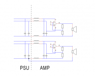
Here's how the audio signal path is routed in my current chip amps.
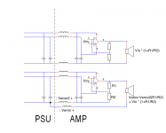
That's a step better than Mark's suggestion, but it can be further improved. See attached.
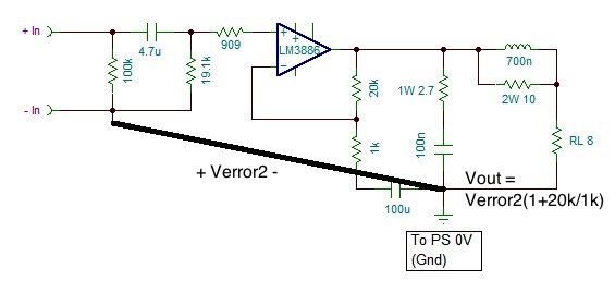
If you hook the input ground to the speaker ground terminal as I suggest doing, you'll end up with one error term:
Vout = Verror2 * (1+R1/R2).
(1+R1/R2) is the gain of the amplifier. Verror2 is the error caused by the current flowing from the input ground (GND_SIG) to the reference ground (GND_LOAD).
Verror2 = Iin * Zground
Iin is the input ground current. We can't really do much to change that, but we do control the ground impedance, Zground. To minimize Zground use a ground plane (jump back a few posts for the explanation).
Also note that the input current is tiny, so Verror2 is pretty darn small to begin with. You can measure the difference between using a ground plane and using a trace in the THD of the overall amp, though.
Tom
Attachments
Last edited:
OK, this is getting interesting now. I like this kind of conversation.
Tom, your assertion again that a ground plane is going to minimize Zground may be true, but if Iin is small what is the real need for that? Under my scenario, only small signal currents are flowing in the PCB ground there doesn't seem to be a need for an especially low Zground.
Regarding two error terms versus one, it's not the number of terms that is important. I assert that your scenario of one error term where all currents are lumped into that is not theoretically better than the situation with two error terms. It all depends on the magnitude of these errors.
So perhaps it comes down to whether the Verror2 introduced by the additional wires in my suggested approach, yet which may reduce Verror1, is an improvement over a single Verror term that might be higher depending on how well the ground plane or other grounding architecture limits the error from the speaker return current.
Does that sound fair?
Tom, your assertion again that a ground plane is going to minimize Zground may be true, but if Iin is small what is the real need for that?
As I mentioned in my post just above: I have measured the degradation in THD from using a trace rather than a plane on the input ground.
Which is better?
Verror2 = [large] * Iin
or
Verror2 = [small] * Iin
If your goal is to get the best performance out of the chipamp that you can, why would you purposely increase the output error signal? You pay the same for the board whether you draw traces or planes, so why not put the copper to good use rather than letting it disappear in the etching process?
Under my scenario, only small signal currents are flowing in the PCB ground there doesn't seem to be a need for an especially low Zground.
Unless your PCB manufacturer or wire vendor offers copper that is superconductive at room temperature, you're increasing the error with your scenario.
Regarding two error terms versus one, it's not the number of terms that is important. I assert that your scenario of one error term where all currents are lumped into that is not theoretically better than the situation with two error terms. It all depends on the magnitude of these errors.
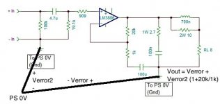
I didn't lump anything together. I reduced Verror to zero by moving the ground reference to the load ground terminal.
If you want the full equation, Vout = Verror + Verror2 (1+R1/R2) is still valid. By moving the ground reference to the output ground, Verror becomes zero and the equation reduces to,
Vout = Verror2 (1+R1/R2).
Does that sound fair?
It sounds like you need to do a bit more analysis. Set it up in a circuit simulator and play with it if that helps. You can see my simulation schematic here:
LM3886 chip amp grounding.
If your goal is to get the best out of the chipamp as possible, the error terms need to be reduced as much as possible. I hope we agree there. If we don't, then I'm not the person to talk to really... I develop precision amps. I don't see any point in reducing only some error terms when reducing the others as well is a simple matter of drawing a few well-placed polygons in a CAD tool. Others are free to disagree with my approach, naturally.
Tom
Last edited:
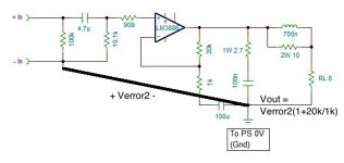
This figure says it all:
The induced voltage from the speaker return ground will influence the small signal 0V voltage and this is magnified by the amp gain.
One of my motivations for trying the approach I am suggesting (separate spkr return to PS 0V and small signal return to PS 0V) is to keep the input ground as quiet as possible. Am I misguided in that kind of thinking?
Also, how about the case of an inverting amp, where there is no ground return for the input? In that case it would appear that all of this is moot.
Regarding two error terms versus one, it's not the number of terms that is important. I assert that your scenario of one error term where all currents are lumped into that is not theoretically better than the situation with two error terms. It all depends on the magnitude of these errors.
Its two error terms versus non as Tom demonstrated in the edited schematic post#24.
Oversized output filter:
An externally hosted image should be here but it was not working when we last tested it.
Simplifying things: Finding a 1K//28K resistor
An externally hosted image should be here but it was not working when we last tested it.
Output filter to scale:
An externally hosted image should be here but it was not working when we last tested it.
You should have approx. 15 turns in order to get enough inductance and that is around 1 uH.
I don't dispute that you measured that, or that the ground plane was better, but I bet that was with the speaker return current running through the PCB ground, right? Take that off of the PCB and then what is the difference you measure?As I mentioned in my post just above: I have measured the degradation in THD from using a trace rather than a plane on the input ground.
See my post above. It's adding another error term but should also reduce the small signal (input) error (at least that is what I assume). Also, the ground reference of the feedback network could be connected to the small signal ground. Why is this not seen? In my approach I am trying to separate ground returns with large currents from those carrying small currents. This is not a good idea?If your goal is to get the best performance out of the chipamp that you can, why would you purposely increase the output error signal? You pay the same for the board whether you draw traces or planes, so why not put the copper to good use rather than letting it disappear in the etching process?
Unless your PCB manufacturer or wire vendor offers copper that is superconductive at room temperature, you're increasing the error with your scenario.
Would not my approach reduce Verror2 significantly even if Verror appears?I didn't lump anything together. I reduced Verror to zero by moving the ground reference to the load ground terminal.
If you want the full equation, Vout = Verror + Verror2 (1+R1/R2) is still valid. By moving the ground reference to the output ground, Verror becomes zero and the equation reduces to,
Vout = Verror2 (1+R1/R2).
It sounds like you need to do a bit more analysis. Set it up in a circuit simulator and play with it if that helps. You can see my simulation schematic here:
LM3886 chip amp grounding.
If your goal is to get the best out of the chipamp as possible, the error terms need to be reduced as much as possible. I hope we agree there. If we don't, then I'm not the person to talk to really... I develop precision amps. I don't see any point in reducing only some error terms when reducing the others as well is a simple matter of drawing a few well-placed polygons in a CAD tool. Others are free to disagree with my approach, naturally.
Tom
For people who are not familiar with how to properly implement a ground plane, or who already have PCBs that lack a ground plane that they want to make the best out of, knowing the sources of error and design choices that lead to increases in THD, noise, and hum pickup is invaluable. Thanks for showing this.
I have implemented my "separate ground return" before and I did not see a significant degradation in THD or other problems. I should probably go back and study this again and do some more measurements. Also your advice to sim the circuit included resistances for traces and wires is a good one, however, what to use for those values is not always clear to me so I would probably just build and measure.
I'll leave it at that.
Its two error terms versus non as Tom demonstrated in the edited schematic post#24.
If you meant "none" by "non" then you are WRONG. There is still the error term on the input, Verror2. I am arguing that Verror2 will be smaller under my scheme, even though another term, Verror, appears, such that Verror and Verror2 together are less than Verror2 for the case of a PCB ground plane but single return from PCB to PS 0V. This is what I am asserting, and what I have not seen any evidence (e.g. measurements or modeling) proving or disproving.
I am simply making an assertion for the different spkr return routing based on the concept that separating high current returns and low current returns will be "better".
Here is the schematic of the star with trace inductions.
The GND is the OUT-
If i'm correct the current trough the large inductor (L1) is Vin / 965ohm
That would be a mA.
But what the effect is on the performance? I don't know. As far as i know, that resistor is for having a 0mv offset.
The GND is the OUT-
An externally hosted image should be here but it was not working when we last tested it.
If i'm correct the current trough the large inductor (L1) is Vin / 965ohm
That would be a mA.
But what the effect is on the performance? I don't know. As far as i know, that resistor is for having a 0mv offset.
Last edited:
Here is the schematic of the star with trace inductions.
The GND is the OUT-

If i'm correct the current trough the large inductor (L1) is Vin / 965ohm
That would be a mA.
But what the effect is on the performance? I don't know. As far as i know, that resistor is for having a 0mv offset.
Why are L4 and L5 paralleled?

CharlieLaub, where am I wrong? The first example has no Verror. All you need to do is connect the input ground so that you do not add an additional error.
Tom explained it in this post (see his two figures that show the Verror and Verror2 terms):
http://www.diyaudio.com/forums/chip-amps/292224-4ch-chipamp-questions-3.html#post4751312
Unless the two of you were talking about different things... I was referring to Toms post when I said that you were "wrong" about no error term since he shows one.
I use both layers for almost all connections.Why are L4 and L5 paralleled?
If you meant "none" by "non" then you are WRONG. There is still the error term on the input, Verror2. I am arguing that Verror2 will be smaller under my scheme, even though another term, Verror, appears, such that Verror and Verror2 together are less than Verror2 for the case of a PCB ground plane but single return from PCB to PS 0V.
You're arguing that the voltage drop caused by a small but finite and non-zero current will be smaller if the conductor has higher resistance. That doesn't match Ohm's law and I'm pretty sure Mr. Ohm is correct.
You are correct that the current is small in the input circuit, so the error term is small. If your goal is to make it as small as possible, you should reduce the impedance of the ground connection. If you are starting from a clean slate, there is no penalty for drawing the input ground as a pour. If you're trying to hack an existing layout, that's another story.
In case of the OP, there is no PCB at this point, right? There's a layout in the CAD tool. Aside from time, there's really no cost to changing the layout at this time, right? I'm assuming OP wants constructive input on his layout rather than a default yes to avoid discussion about how to improve the layout.
This is what I am asserting, and what I have not seen any evidence (e.g. measurements or modeling) proving or disproving.
Considering that this is DIY Audio and not Federal Court, I'm not sure I can prove, disprove, or show legal evidence. Here's some data on LM3886 grounding that I published over two years ago: http://www.diyaudio.com/forums/chip-amps/252436-lm3886-pcb-vs-point-point-data-3.html#post3846783
I am simply making an assertion for the different spkr return routing based on the concept that separating high current returns and low current returns will be "better".
No argument there. One way to do that is to join GND_SIG and GND_LOAD at the speaker return connection. I'm not aware of any way that's better.
Here is the schematic of the star with trace inductions.
I suggest including the trace resistances as well.
I use both layers for almost all connections.
Except the input and feedback ground...
")
Tom
I suggest including the trace resistances as well.
Except the input and feedback ground...
Tom
I Will add the values.
But i figured that if the trace resistance is only 0.01222 Ohms for the feedback resistor trace. (On a 1mA current and 965Ohm resistor trace). Would that trace resistance be not important.
Only the mute and Compensation Resistor ground uses 1 layer.
You call it FB gnd, but is it an active part on the Feedback network?
You should have approx. 15 turns in order to get enough inductance and that is around 1 uH.
I used coil32 to calculate the amount of windings for a 0,7uH induction
it came op with 5,5 windings for a diameter of 28mm and a 2.5mm wire.
Maybe i filled in something wrong?
- Status
- This old topic is closed. If you want to reopen this topic, contact a moderator using the "Report Post" button.
- Home
- Amplifiers
- Chip Amps
- 4ch Chipamp questions