I ordered this item from ebay, but the seller (as usual) does not automatically send the schematic to me. when I asked for it, the seller claims to not understand the word 'schematic'. sheesh!
can someone help me? if anyone has bought this item (it seems to be from many sellers) and can send me the pdf schematic, that would be much appreciated.
item is:
TPA6120A Headphone Amplifier Board NE5534 DIY Amp | eBay
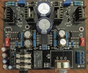
photo:

can someone help me? if anyone has bought this item (it seems to be from many sellers) and can send me the pdf schematic, that would be much appreciated.
item is:
TPA6120A Headphone Amplifier Board NE5534 DIY Amp | eBay
photo:

I'm a little afraid to run it! some parts got VERY hot during a few minutes time and without a design doc, I can't know this is was competantly designed or not.
it seems none of the sellers are willing or able to release the schematic. I should have asked that first before buying (damn, got burned yet again from ebay/china).
what I'll probably do is to take some high res top and bottom board photos, at least as a starting point.
my thoughts, at this point, are to assume the design is crap and to remove all parts that are not essential. redo the psu, remove the op-amps (what are they there for, anyway?) and just drive the chip in its databook recommended way.
so many psu's from china run very hot. I strongly disagree with that concept; and when the pcb got too hot to handle (I think it might be some low value resistors burning) I turned it off and didn't power it on or risk my good phones any further.
maybe this IS a good design, but with the heat thrown off, I'm just not convinced.
I would not recommend anyone buy this until we get to the bottom of it. I've heard good things (on paper) about this TI chip (btw, its NOT toshiba; would it really have hurt the sellers to at least CHECK their ad copy? nikon caps? really? are they wide-angle or telephoto LOL!)
The op-amps are a gain stage preceding the 6120.
I would probably forget about the p.s. on the board as well and just use a power supply on a separate board.
The on-board p.s. looks like some type of shunt regulated supply, but I could be wrong.
I know for a fact the 6120 can sound really good if implemented properly.
I would probably forget about the p.s. on the board as well and just use a power supply on a separate board.
The on-board p.s. looks like some type of shunt regulated supply, but I could be wrong.
I know for a fact the 6120 can sound really good if implemented properly.
I mostly wanted a premounted 6120 since its a bit hard to diy, and the chip really needs a non-perfboard setup, too. I usually do my own perfs but this chip is a bit fussier, from what I've heard.
yes, the psu is a shunt. the ebay/china guys seem to like high-heat shunts (sigh). I don't understand it; they run so hot, are quite inefficient and I'm not aware that they are lower noise than even 317 series regs. the phones amp chip is not that power hungry, so I'm at a loss to understand the rationale behind this ultra hot running psu. I actually smelled something bad when it got so hot, that's another reason I turned it right off.
as for the gain stage, why is that needed? shouldn't a 2v dac be enough to drive this? the datasheets dont' show any sample circuits with prebuffering; so I'm not sure why local prebuffering is needed.
what I WOULD like, to a small degree, is a servo - since this is known to be a little bit high on the dc offset side. but again, the TI sheets dont' show a servo and its probably 'fine' to run without one; but I know some designs do servo the output to null it better.
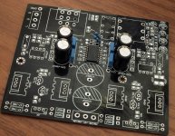
I made some progress today. I removed the entire psu parts set, the entire op-amp pre-buffer set and the connectors, too. everything except the chip and its direct gain-setting smd resistors (1k and 1k) and the semi local bypasses and filters (.1 and some larger bulk can).
I have not traced thru the whole thing yet, but the key parts that I can see are that they are using a single ended non-inverting config; figure 14 in the datasheet that I have. but, the data sheet shows 39.2ohm series output resistor and all the china schematics I can find on GIS search show 10ohms. TI says it can be as low as 10, but why ever take a 'as low as' figure in your design? I took off the 2 10's (thruhole) and I'll try 40 or so, whatever I can get close to that. figure 14 in the spec sheet also shows 50ohm series Rs on the non-inverting input of the amp section. I did see a 47ohm smd R under the board, from the output of the op-amp prebuffers, so that's cool, they followed the spec there")
what I've also gleaned is that this chip does not like variable Z going into it. I think that's why you don't see many pots or attens thrown right onto the input of this phones chip. you see attens, then OA buffers, then you see this chip. so, I now 'get' why there were ne5534's on this board. the screening actually says opa627, but that's just wishful thinking
each channel (left and right) on the TI chip gets its own bipolar supply. that's why there are 4 transistors in heatsinks (A940 is what is marked, I think that means 2SA940, which is a pnp power?)
there are 4 tl431 3-pin chips between the heatsinked a940 transistors. I think those are voltage refs of some kind. the trimmer would set the output voltage. oh, and the resistors that got hot are 47ohms, maybe 1/2w size but they were really hot the short time I had this thing powered on. maybe it was oscillating and maybe that power draw was not normal.
I snapped some top and bottom pics before I started tearing into the board to remove all but the phones amp chip and its bypass/bulks, plus the 2 1k's that are the gain programming (Rf and Ri) resistors.
I'll figure out what kind of dual 10 or dual 12 supply I'll give this. but it aint gonna be what came on the board, that's for sure
I'm also a bit fearful of output offset. if I can put together a dummy load, I'll see what the offset ends up being from music and test signals. the whole thing is not worth a thing if its offset is too high (pcb layout can affect that, so that's one thing that's a constant and I can't change).
update: photos included
I have not traced thru the whole thing yet, but the key parts that I can see are that they are using a single ended non-inverting config; figure 14 in the datasheet that I have. but, the data sheet shows 39.2ohm series output resistor and all the china schematics I can find on GIS search show 10ohms. TI says it can be as low as 10, but why ever take a 'as low as' figure in your design? I took off the 2 10's (thruhole) and I'll try 40 or so, whatever I can get close to that. figure 14 in the spec sheet also shows 50ohm series Rs on the non-inverting input of the amp section. I did see a 47ohm smd R under the board, from the output of the op-amp prebuffers, so that's cool, they followed the spec there
what I've also gleaned is that this chip does not like variable Z going into it. I think that's why you don't see many pots or attens thrown right onto the input of this phones chip. you see attens, then OA buffers, then you see this chip. so, I now 'get' why there were ne5534's on this board. the screening actually says opa627, but that's just wishful thinking
each channel (left and right) on the TI chip gets its own bipolar supply. that's why there are 4 transistors in heatsinks (A940 is what is marked, I think that means 2SA940, which is a pnp power?)
there are 4 tl431 3-pin chips between the heatsinked a940 transistors. I think those are voltage refs of some kind. the trimmer would set the output voltage. oh, and the resistors that got hot are 47ohms, maybe 1/2w size but they were really hot the short time I had this thing powered on. maybe it was oscillating and maybe that power draw was not normal.
I snapped some top and bottom pics before I started tearing into the board to remove all but the phones amp chip and its bypass/bulks, plus the 2 1k's that are the gain programming (Rf and Ri) resistors.
I'll figure out what kind of dual 10 or dual 12 supply I'll give this. but it aint gonna be what came on the board, that's for sure
I'm also a bit fearful of output offset. if I can put together a dummy load, I'll see what the offset ends up being from music and test signals. the whole thing is not worth a thing if its offset is too high (pcb layout can affect that, so that's one thing that's a constant and I can't change).
update: photos included
Attachments
Last edited:
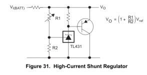
that seems about right, from the casual look I gave the PSU section.
is there anything really great about this topology? why use it if, say, 317/337 may be good enough or even better? this is not a high current application, I don't think (btw, what is the current draw on this, in normal use? just a range would be useful in helping me pick out a supply for this. I have an eval TI psu reg board that is really low noise and low heat, but not a lot of current from it. not sure what this board is really going to need if I'm driving a senn 580/600/650 style can.
is there anything really great about this topology? why use it if, say, 317/337 may be good enough or even better? this is not a high current application, I don't think (btw, what is the current draw on this, in normal use? just a range would be useful in helping me pick out a supply for this. I have an eval TI psu reg board that is really low noise and low heat, but not a lot of current from it. not sure what this board is really going to need if I'm driving a senn 580/600/650 style can.
and the relay and protection chip, I cut that stuff out since its some weird chip (to me) and I don't see it as something that is easy to buy or work with, so it seemed ditch-able. I have controllers that can do muting on power on and off, so their circuit is not needed. otoh, if their circuit did dc offset detection, that would have been useful
at some point, I may even just physically cut the board with some area around the chip but not much else (leaving room for mounting holes). an expensive, labor-intensive 'chip carrier' of sorts, lol. (sigh...)
at some point, I may even just physically cut the board with some area around the chip but not much else (leaving room for mounting holes). an expensive, labor-intensive 'chip carrier' of sorts, lol. (sigh...)
Some people on here really obsess over low impedance and overly complicated power supplies. I'm not one of them.
Personally, I've used a $25 317/337 supply from China for about 4 years now and have never had any noise issues with any buffer/preamps that I've built.
Keep in mind I don't do phono or other high-gain amplifiers, though.
You can use a resistor as low as 10 ohms on the outputs of the 6120, but I use 49.9 Vishay SMD resistors only because my boards use only SMD's around the 6120.
Also, it's a known fact that DC offset will be high with many current-feedback amplifiers(or with voltage-feedback amplifiers with high input bias currents such as the AD797, AD827, LM6172, etc.). As you figured out, they do not like varying input impedance from "hanging a volume pot" on the front of them.
With only a gain of 2, offset with the 6120 usually isn't too bad, but I would still put another op-amp in front of the 6120 and place the volume pot in front of it.
Just be sure and measure the offset before connecting your phones.
the decoupling caps are the blue boxes next to the electrolytics.
I think they are too far away. I noticed that immediately.
do you think I'll run into osc problems with where they are, now?
typical ebay/china board. some day, I'll learn not to even try these bad designs/implementations anymore. almost every one I buy to try out, they have major problems in one area or another ;(
btw, what I'm thinking of doing, for a prebufer, is to use a PGA vol control chip or cirrus equiv. those all contain low-z output buffers which would be fine enough to drive the input of this phones amp. I can see that if you are going to throw a passive pot or stepped atten before this, you should prebufffer; but the active vol controls already have a post-buffer on them.
do you think I'll run into osc problems with where they are, now?
Maybe, maybe not. It would be worth checking on a scope at least. What's also worth checking is what they used at the output. 10r resistors ?
I have some TPA6120 carrier boards that I have designed so that I can play with that chip. They are configured in a single-ended non-inverting config. You are more than welcome to one if you want it. Or, I can post the schematic/PCB files for Eagle and you can have them printed whenever you need them.
I have a hot air station and do TONS of work with these chips. I have one of my amps in another thread here. If you don't like soldering this chip (due to the TP on the bottom), you can send me your chip and I'll send it back soldered to the board. Let me know if you want one and PM me your info.
I have a hot air station and do TONS of work with these chips. I have one of my amps in another thread here. If you don't like soldering this chip (due to the TP on the bottom), you can send me your chip and I'll send it back soldered to the board. Let me know if you want one and PM me your info.
- Status
- This old topic is closed. If you want to reopen this topic, contact a moderator using the "Report Post" button.
- Home
- Amplifiers
- Headphone Systems
- schematic request for tpa6120/ne5534 ebay amp