I don't even see the problem, and the reason of all the 'noise' about this, like symmetrical VS asymmetrical, speed of the OPS etc...The mistake we made earlier in this thread was to say you have to close the loop at the same frequency as VFA because of the OPS phase shift, which is in this 1-3 MHz range where in a VFA you get a decent PM. As you pointed out earlier, the additional gain stages in a VFA cause the additional phase shift. You dont have those in a CFA so you can close a CFA loop at a higher frequency, and get the benefits.
And Apples/oranges comparisons.
THE ONLY DIFFERENCE between VFA and CFA lie in the INPUT STAGE where feedback is applied.
VFA usually use LTP, witch add an active device, as you say, in the feedback path. This add phase turn at HF with all its consequences.
There is no reason why we cannot add gain, stages, etc... to a CFA. We chose our poison: More gain -> less distortion at low frequencies, reduced open loop bandwidth.
As far as i'm in concern, my goal , to reproduce a 20Khz bandwidth, is to try to get a constant feedback ratio in the bandwidth, means an open loop bandwidth up to 20KHz.
When it is about low frequencies (above 1KHz), as in an active multi-way system, i do not care about VFA or CFA. And prefer VFAs because it is easyer (more simple) to get high linear feedback ratio (less distortion) in the requested bandwidth.
If we need 20KHz, i prefer CFAs, because they can go higher and harmonics matters.
Last edited:
That is exactly how prof. leach did it. Read about WHY he did it that way.
For a CFA , it is "the lesser of two evils" ...
OS
OS - can you point me to which of his docs discusses that?
That's generally true for most implementations, but for me the interesting part comes from thinking about why.It's very clear in my view. High loop gain precision go for VFA. High speed wide band go for CFA
High slew rate designs (typically CFA)
The high slew rate capability can be mostly attributed to the combination of a symetrical design and an input stage offering biderectional current-on-demand. Unfortunately the current gain of the VAS is normally severely limited to ensure stability of the VAS idling current, and this results in low open loop gain.
Those attributes and compromises can also be had with a VFA, e.g. using John Curl's preferred topology.
High open loop gain designs (typically VFA)
Here a single-ended VAS is used so it can have high current gain without causing any problems, and this results in high open loop gain. Unfortunately the input stage normally does not offer biderectional current-on-demand, so very high slew rates can't be achieved.
Those attributes and compromises can also be achieved with asymetric CFAs, e.g. by using the Quad303 topology or similar.
Not all amps fall into one of those two categories though. For example, to get the worst of both worlds, go for a symetrical design with a low current gain VAS and an input stage comprising two independent LTPs.
Sure. To get the best of both worlds, use a symetrical topology with the following:the big question then is how to design either one so that advantages or disadvantage are equalized...
is that even possible?
a) An input stage capable of biderectional current-on-demand. (for high slew rate)
b) A push-pull VAS with high current gain. (for high open-loop gain)
c) Common mode feedback to stabilise the VAS quiescent currents.
d) Ideally, the VAS should also provide biderectional current-on-demand without hard crossover distortion, so it doesn't become the weak link.
It's not overly challenging to design something like that, but the CMFB does add some complexity. When I was last home a couple of days ago, I was playing with a proof-of-concept circuit in simulation and there didn't seem to be any problems. When I get back, I'll post a schematic.
In a nutshell, it used a feedback circuit that sets (Ivas1 * Ivas2) = (Iinp1 + Iinp2) * N where:
- Ivas1 and Ivas2 are the collector currents of the two VAS transistors
- Iinp1 and Iinp2 are the output currents from the input stage
- N was about 5 or 10, I forget, but it's easy to adjust.
To be more clear about the consequences of the added active device ( in LTP ) feedback path, for those who are not familiar to this.
Because the transition frequency of this transistor is not infinite, it will produce phase turn at high frequencies.
Because the original signal and the feedback signal are no more in perfect phase, the subtraction result will not be perfect. The overall gain will begin to increase at HF. This lead to instability as well as increase of distortion. So, we are obliged to compensate with a Miller (or equivalent) to flatten the closed loop, reducing the open loop bandwidth, with no help on distortion...
You will say: Ok, let's use the LTP in inverting configuration. This way, the feedback and the original signals are subtracted passively, no FT, no active device in the feedback path.
That's right. But, then, we face an other problem. Because the base of the inverting transistor present a parasitic capacitance, we need to operate at low feedback impedance for no feedback phase turn because of this RC filter. Too low, in practice, for a usable input impedance in a power amplifier. While, in a CFA, we can make the feedback impedance as low as we want to face the parasitic capacitances of the input transistor emitter, keeping the base input at a nice impedance value.
Yes, CFA at HF is a private club where Murphy has no entrance card.
Last edited:
I don't even see the problem, and the reason of all the 'noise' about this, like symmetrical VS asymmetrical, speed of the OPS etc...
The problem was that they were told but didnt like to be.

...
Now, i use those OP260 in my personal preamp and everywhere i can in all the analog stage of my hifi system. ...
The Analog Devices website lists the OP260 as "obsolete product" (out of production)
and suggests AD812 as replacement part. Do you have any experience with those ?
Oh ! What did-you say ?
Murphy has find a way to spoil our nights, making noise via our too thin back door (what you call "power supply ripple rejection").
Hehe, just kill the problem at its source, building a wall between us and him: Ripple filters. Happily, we can achieve-it by filtering only low currents input+VAS stages... so cheap and easy
Last edited:
Sadly, the requested feedback impedance of the AD812 is much lower for the same performance :-(The Analog Devices website lists the OP260 as "obsolete product" (out of production)
and suggests AD812 as replacement part. Do you have any experience with those ?
Not exactly a replacement part !!!
(I could kill them ;-)
I found microwave devices to be very linear. Especially those designed for class A single-ended operation.
I see this kind of estimates, every day and every night in the pseudo-engineering language of DIY. What the hell is "more linear", "very linear", etc... when it comes to active devices? How and why is a microwave device "more linear" that the next device in the junk box? How was this "more linearity" determined?
This is to me like saying that thick cables sound "fat", silver wiring sound "silvery" and copper wiring sound "tarnished".
The mistake we made earlier in this thread was to say you have to close the loop at the same frequency as VFA because of the OPS phase shift, which is in this 1-3 MHz range where in a VFA you get a decent PM. As you pointed out earlier, the additional gain stages in a VFA cause the additional phase shift. You dont have those in a CFA so you can close a CFA loop at a higher frequency, and get the benefits.
Closing the loop at the same frequency was considered a practical limitation. I still have to see a high power amplifier with an ULGF of 5-6MHz outside the simulator.
Otherwise, if you prefer to look from this perspective, you need to push the CFA ULGF at higher frequencies just to get the same loop gain as in the VFA, hence the same degree of linearity when closing the loop. That's the classic gain vs. bandwidth trade, and why would one risk using a higher ULGF?
Yes, I know, there's always the "open loop bandwidth" fallacy at the rescue.
the worst of both worlds
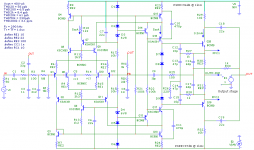
Please take a look at the front-end shown below. Two LTPs and two TISes with a low current gain of just 1x. Nevertheless, it slews pretty high, 500V/us and distorts 61ppb at 20kHz. Exceptio probat regulum.
A constant product rule, on the other hand, might have the advantage that none of the VASes will completely turned off during overload conditions.
Cheers, E.
[..]
For example, to get the worst of both worlds, go for a symetrical design with a low current gain VAS and an input stage comprising two independent LTPs.
Please take a look at the front-end shown below. Two LTPs and two TISes with a low current gain of just 1x. Nevertheless, it slews pretty high, 500V/us and distorts 61ppb at 20kHz. Exceptio probat regulum.
Why, for heaven's sake, keeping the product (Ivas1 * Ivas2) constant, instead of the sum (Ivas1 + Ivas2)? As for the latter, it already has been done with only four extra BJTs. Have a look at the MCP amp. BTW, this amp comprises two CFB stages.It's not overly challenging to design something like that, but the CMFB does add some complexity. When I was last home a couple of days ago, I was playing with a proof-of-concept circuit in simulation and there didn't seem to be any problems. When I get back, I'll post a schematic.
In a nutshell, it used a feedback circuit that sets (Ivas1 * Ivas2) = (Iinp1 + Iinp2) * N where:
- Ivas1 and Ivas2 are the collector currents of the two VAS transistors
- Iinp1 and Iinp2 are the output currents from the input stage
- N was about 5 or 10, I forget, but it's easy to adjust.
A constant product rule, on the other hand, might have the advantage that none of the VASes will completely turned off during overload conditions.
Cheers, E.
Attachments
To be more clear about the consequences of the added active device ( in LTP ) feedback path, for those who are not familiar to this.
Because the transition frequency of this transistor is not infinite, it will produce phase turn at high frequencies.
Because the original signal and the feedback signal are no more in perfect phase, the subtraction result will not be perfect. The overall gain will begin to increase at HF. This lead to instability as well as increase of distortion. So, we are obliged to compensate with a Miller (or equivalent) to flatten the closed loop, reducing the open loop bandwidth, with no help on distortion...
You will say: Ok, let's use the LTP in inverting configuration. This way, the feedback and the original signals are subtracted passively, no FT, no active device in the feedback path.
That's right. But, then, we face an other problem. Because the base of the inverting transistor present a parasitic capacitance, we need to operate at low feedback impedance for no feedback phase turn because of this RC filter. Too low, in practice, for a usable input impedance in a power amplifier. While, in a CFA, we can make the feedback impedance as low as we want to face the parasitic capacitances of the input transistor emitter, keeping the base input at a nice impedance value.
The sum of all misconception about negative feedback: feedback is slow and is chasing it's tail (actually a confusion between group and phase delay).
The rest is the usual technobabble denoting the lack of an elementary understanding of fundamental concepts: Miller compensation (reduces HF distortion even without closing the global feedback loop), active devices nonlinearities and parasitic elements (parasitic capacitances of active devices are the same whatever topology you are using, and their effect has nothing to do with the feedback), etc... to many to even bother understanding...
Happy listening and hope your audio company goes well.
Fair enough.Please take a look at the front-end shown below.... Exceptio probat regulum.
Yes, that was the idea. It allows VAS output current greater than double the quiescent current, without a sudden transition where one device switches off and the other is obliged to double it's incremental gain. The downside is that it introduces a small amount of 2'nd harmonic distortion if the open loop gains of the two sides aren't matched. So it's basically a trade-off, trying to choose the lesser of two evils.Why, for heaven's sake, keeping the product (Ivas1 * Ivas2) constant, instead of the sum (Ivas1 + Ivas2)?
[snip]
A constant product rule, on the other hand, might have the advantage that none of the VASes will completely turned off during overload conditions.
Having a look now. Thanks.Have a look at the MCP amp. BTW, this amp comprises two CFB stages.
Hi Kris,
Which circuit, the MCP amp or the SuperTIS?
Could you comment on both please... Does it have to be a SMD?
Hi Kris,Could you comment on both please... Does it have to be a SMD?
I believe that Paul (mcd99uk) has built the MCP amp, or at least something having a lot in common. As for the Super TIS, this one has not been built yet. No SMDs are required.
Cheers, E.
CMFB/CMCL
Thanks for explanation (and I agree with your reasoning). Next point: how many additional BJTs are required for a constant product CMCL?
Cheers, E.
[..]
Yes, that was the idea. It allows VAS output current greater than double the quiescent current, without a sudden transition where one device switches off and the other is obliged to double it's incremental gain. The downside is that it introduces a small amount of 2'nd harmonic distortion if the open loop gains of the two sides aren't matched. So it's basically a trade-off, trying to choose the lesser of two evils.
[..]
Thanks for explanation (and I agree with your reasoning). Next point: how many additional BJTs are required for a constant product CMCL?
Cheers, E.
I've rewritten the CFA vs VFA doc and posted it up on my site - link below.
CFA vs. VFA Amplifiers: a Short Primer
CFA vs. VFA Amplifiers: a Short Primer
- Home
- Amplifiers
- Solid State
- CFA Topology Audio Amplifiers