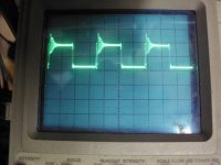
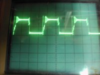
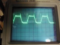
All pics with ~75w load. Scope probe on outer primary leg.
Pic 1: ~10v input. Mosfets cool.
Pic 2: ~13v input. Regulator starting to reduce PWM. Minimal heating of mosfets.
Pic 3: ~15v input. PWM reduced further. Mosfets hot.
Pic 1: ~10v input. Mosfets cool.
Pic 2: ~13v input. Regulator starting to reduce PWM. Minimal heating of mosfets.
Pic 3: ~15v input. PWM reduced further. Mosfets hot.
Attachments
lazzer, your pcb layout needs to be improved wrt the fet drive loop and where the IC gnd connects to the main power ground. The fet gate drive current loop needs to be a minimum loop path, not a large loop path that includes the main switchmode current paths. The IC should gets its reference voltage gnd, and fet drive gnd from the a star point that also stars to the main filter caps (ie. over near the FET sources.
What frequency are you switching at? You may want to also add some smt ceramics on the rear of the pcb to provide minimised loops for the higher frequency components of the waveforms.
Are your measured results from that pcb, or a birdsnest?
Ciao, Tim
What frequency are you switching at? You may want to also add some smt ceramics on the rear of the pcb to provide minimised loops for the higher frequency components of the waveforms.
Are your measured results from that pcb, or a birdsnest?
Ciao, Tim
Before you go any further, read Jim Williams application note AN118 on high voltage SMPS;
http://cds.linear.com/docs/en/application-note/an118fa.pdf SMPS design is not trivial, and secondary voltages which you seek require a belt and suspenders approach to transformer wire insulation and insulation between layers.
You're going to blow the trace between the sources of the MOSFETs shown on your PCB. Don't be afraid of using both sides of the PCB, but try to keep the high current traces continuous, i.e. without via's -- you can easily route the gate drive resistors such that they jump the high current traces.
In testing any power supply, it's helpful to have a transistor radio nearby (and ON!) -- wonderful for letting you know if there's a problem!
lazzer, your pcb layout needs to be improved wrt the fet drive loop and where the IC gnd connects to the main power ground. The fet gate drive current loop needs to be a minimum loop path, not a large loop path that includes the main switchmode current paths. The IC should gets its reference voltage gnd, and fet drive gnd from the a star point that also stars to the main filter caps (ie. over near the FET sources.
What frequency are you switching at? You may want to also add some smt ceramics on the rear of the pcb to provide minimised loops for the higher frequency components of the waveforms.
Are your measured results from that pcb, or a birdsnest?
Ciao, Tim
I'm testing the circuit on a PCB. I'll re-arrange things and see if it helps. My gate waveform looks decent with fast rise and fall times with slight ringing after turn on. It works great when PWM is full (~49%) but as soon as it reduces the width it gets hot.
Before you go any further, read Jim Williams application note AN118 on high voltage SMPS;
http://cds.linear.com/docs/en/application-note/an118fa.pdf SMPS design is not trivial, and secondary voltages which you seek require a belt and suspenders approach to transformer wire insulation and insulation between layers.
You're going to blow the trace between the sources of the MOSFETs shown on your PCB. Don't be afraid of using both sides of the PCB, but try to keep the high current traces continuous, i.e. without via's -- you can easily route the gate drive resistors such that they jump the high current traces.
In testing any power supply, it's helpful to have a transistor radio nearby (and ON!) -- wonderful for letting you know if there's a problem!
The yellow line between sources? It's a jumper. PCB is single-sided to make prototyping easier. The large traces are covered in a thick layer of solder. PCB stays cool. Probing along the ground trace shows minimal noise through trace.
Thanks. I'll give it a read. What is a belt and suspenders approach? My bobbin isn't large enough to wind a belt and suspenders.

I like the radio idea.
How do car audio amplifiers seemingly just slap together a minimalist power supply (with long drive traces weaving through long power stage traces and the component side littered with the components) yet it works fairly efficiently? I even rewound one for 400v and it worked fine. They are unregulated though. Maybe regulation isn't the way to go about this.
Last edited:
Efficiency is based around understanding where the losses are, and routing circuits so that important parasitics are managed.
It is important to have a design prepared, where all operating parameters (at idle and max power) are identified, including peak current levels and voltage drops and power dissipations, and relating them to the parts choice and the transformer design. If people can't review that design detail, then it pushes the design role on to others wrt part selection, such as your diode selection query, and raises so many question marks as to whether basic parts such as the transformer have a suitable design. Everything in a switchmode tends to interact, so all design aspects need to be looked at in order to get a feel of assurance.
Poor parasitic management shows up in your waveforms, which is why I looked at your pcb grounding scheme. PCBs can have long drive traces weaving all over the place if the basics of star grounding are understood with respect to where all the switching currents are flying around in different loops.
A photo of your measurement technique for the CRO photos is also worthwhile, as the use of anything but short ground stubs as per rf probing techniques can present spurious waveforms at switching transitions that misrepresent what is actually occurring.
I wound 3 transformers (From PC power supply and ETD34 cores I ordered) with various winding techniques on the primary since there's no clean way to wind an ETD core for a CT primary for 12v PP step-up. Transformer one had a primary using twisted parallel wires. Transformer two using untwisted side by side (single layer). Transformer three had them layered on top of each other (two layers).
My secondary I calculated to 160t. #22 fit the bobbin 40 turns per layer. I wound one layer up then back for 80t and grabbed the CT then wound up and back for another 80t. The secondary is wound on top of the primary.
All 3 transformers produced similar results and poor overall efficiency of 75%. I don't think the transformer is the issue but I won't dismiss it.
My scope probe is a little red probe with a 6" lead coming out of the side of it with an alligator clip I've connected to supply ground at the PCB. It has a 3 position slide switch on the side that effects it's sensitivity.
I'll work on a new PCB layout tonight and see about shortening up the high-current paths.
What photo do you need? My "measurement technique" is clipping on the probe ground and probing the traces.
Last edited:
Found the shutdown issue. It was caused by a small voltage leak to the shutdown pin. Looks like the SG3525A has a much lower shutdown voltage then the NTE1721. That reminded me to put the remote turn-on circuit back in which works now.
I'm still trying to learn what the compensation input is for and yes, I've read about it. What is it compensating for, what does it do to compensate, and what is the benefit of compensation? I've seen it wired so many different ways. I pulled the feedback off the comp circuit to see if it had to do with the issue... nope.
I'm still trying to learn what the compensation input is for and yes, I've read about it. What is it compensating for, what does it do to compensate, and what is the benefit of compensation? I've seen it wired so many different ways. I pulled the feedback off the comp circuit to see if it had to do with the issue... nope.
Compensation goes to achieving stability across your operating range with the fastest feedback loop transient response - but that is pretty exotic stuff to put in place as it needs a very well known and settled power supply and techniques for measuring phase margin, and helps if you have a simulation set up.
Assuming your transformer wire size and turns design are fine, then interleaving is your first improvement, and should work well - but you need to include adequate working voltage insulation between pri and sec (at least you don't have to worry about serious insulation). Flat multifilar is good, easy to achieve, and probably gives the best coupling and lowest proximity etc losses for a diy.
It doesn't take much of a noise glitch to move reference and IC levels around. With your existing pcb, you could cut the 0V trace that joins the IC circuitry to the input 0V bus trace, and take an underboard link from pin 12 to the common source of the FETs. And take the output 0V to pin 12.
If you can get any surface mount parts (eg. diodes, bypass caps in at least 1812 size), then making a pcb with lands on the rear to mount a few critical parts is a simple and very effective way to significantly reduce current loop areas and get much cleaner switching and regulation. This would especially work for the diode rectifier section.
A probe spring clip (terminology - What is the name of this springy type oscilloscope probe accessory? - Electrical Engineering Stack Exchange) is your best friend for avoiding seeing lots of glitches that aren't actually there.
Here's one for the SG3525 which should work better:
An externally hosted image should be here but it was not working when we last tested it.
Thanks trobbins. I'll make the connections per your advice and post the results.
jackinnj - That layout seems to have the same problems that trobbins says mine has which is the IC ground being far away from mosfet source pin and your trace between C1a and supply ground seems thin.
jackinnj - That layout seems to have the same problems that trobbins says mine has which is the IC ground being far away from mosfet source pin and your trace between C1a and supply ground seems thin.
Last edited:
I'm currently drawing up a second PCB layout to try to improve things.
I'm considering TO220 diodes but I think that's overkill for my 250ma requirement. There's just SO many diodes out there. For bridge rectification using TO200 I'll need one common anode and one common cathode -OR- a pair of series diodes like these. http://www.mouser.com/ds/2/427/94554-267929.pdf
I'm using the Mouser filters to try and narrow down my choices into the 600v 50ns range but I'm still having a hell of a time narrowing things down from there to something fast and cheap. Should they also be "soft recovery"? What VALUE is "soft"? Soft is an opinion after all, not a value.
I may need a hand calculating my output chokes. The ExcellentIT transformer calculator said I needed 8000uh chokes. That's a lot of choke.
Last edited:
I remember using the ES1x range of smt 1A diodes for small switchmodes using mainly leaded parts - easy to find (eg. at mouser: smt, 600V, 1A, ultra fast filters). They make the layout of Tx former terminals, diodes, smt cap very small, with the above board main electrolytic also very close to the former.
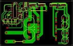
Good on you lazzer. If you wanted to be pedantic, the 0V trace for all the regulator IC parts should go to pin 12 directly, not the filter cap. The trace between that filter cap and pin 12 has the FET gate drive transient on it, which would couple in to all the IC references. I think recent IC's blank that part of the period out from decision making, but the older IC's wouldn't have.
Are you able to move the transformer closer to the power devices (eg. keep the links on the pad side)? The aim being to reduce any high current switching loop area to a minimum.
Are you able to move the transformer closer to the power devices (eg. keep the links on the pad side)? The aim being to reduce any high current switching loop area to a minimum.
I may be able to sneak the grounds up to pin 12 but it might be a squeeze. I'm trying to keep a lot of space in between traces because my friend makes me etching masks out of vinyl. His cutter isn't accurate enough for tiny traces. That's also why it's single layer.
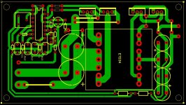
The way this board sits in the chassis requires the heatsink to be placed on the edge of the board. I don't think there's a way to wire the mosfets without jumpers.
Here's an update but I haven't moved the grounds to pin 12. Some of the jumpers like the + supply input and the rectifier outputs have chokes instead. There are no snubbers on the primary. I tried using them on my first board with various values but it didn't help the ringing. I didn't see any large overshooting on the scope and the mosfets are holding up ok. Are snubbers more commonly used on line powered supplies? I don't see them in any of my car amplifiers.
Attachments
Last edited:
No worries about the pcb layout - my comments were only for information, and to assist understanding - we all have to make compromises
Snubbering can be applied for many reasons. Keep It Super Simple (KISS) applies unless there is a need. If the drain voltage was getting close to rated max then that's one reason. If switching loss during a particular transition is substantial and causing thermal stress or the aim was for highest efficiency then it may be minimised with a snubber - but you need to be very aware of what is at play. If the high frequency content of the voltage waveform was coupling to heatsink and chassis and emi is a concern, then that's another reason.
Snubbering can be applied for many reasons. Keep It Super Simple (KISS) applies unless there is a need. If the drain voltage was getting close to rated max then that's one reason. If switching loss during a particular transition is substantial and causing thermal stress or the aim was for highest efficiency then it may be minimised with a snubber - but you need to be very aware of what is at play. If the high frequency content of the voltage waveform was coupling to heatsink and chassis and emi is a concern, then that's another reason.
How about turning the whole transformer 90degrees and having the mosfets on the top like they are now, but put the diodes on the bottom??? Nice and symmetrical - me like...
The power tracks should not get that much longer, but the mosfet drains definitely will get shorter...
I would also move the gate resistors directly at the gates. They can be under the mosfets.
The power tracks should not get that much longer, but the mosfet drains definitely will get shorter...
I would also move the gate resistors directly at the gates. They can be under the mosfets.
This thread made me look for the transformer calculator i had built with the data from a Linear Tech datasheet -- I had to recreate it -- must've been on the old computer:
An externally hosted image should be here but it was not working when we last tested it.
- Status
- This old topic is closed. If you want to reopen this topic, contact a moderator using the "Report Post" button.
- Home
- Amplifiers
- Power Supplies
- SG3524 SMPS help needed.