Its time to PLay --
Random thoughts after visiting this thread --
Its time to Play - Spot the Looney.
I put on clean underwear for This?
STATISTICS: Means never having to say you're certain.
ADMIT IT - Life would be so boring without me.
Unless your name is "Internet", stop acting like you know everything.
Always be yourself.
Unless you suck.
KEEP CALM and PLAY ON
-RNM
")
Random thoughts after visiting this thread --
Its time to Play - Spot the Looney.
I put on clean underwear for This?
STATISTICS: Means never having to say you're certain.
ADMIT IT - Life would be so boring without me.
Unless your name is "Internet", stop acting like you know everything.
Always be yourself.
Unless you suck.
KEEP CALM and PLAY ON
-RNM
<snipped>
BTW the offset issues on that amp are very serious at 48V supply.
That's putting it mildly, maybe.
I have been simulating the Forssell jfet op amp, today (with two ideal superconducting 24V batteries, each being roughly half the size of the universe).
The "offset control" pot doesn't seem to do much of anything. But if I raise R7's value (from 330 to about 518.8 Ohms!), it eliminates the huge DC offset.
There might be a simple explanation, though: The one thing that I seem to be lacking is the three different ranges of device Idss. Would that explain an offset problem? And how important will (the lack of) those be, in a simulation?
Here are the jfet models that I found:
.model J2sk170 NJF(Beta=59.86m Rs=4.151 Rd=4.151 Betatce=-.5 Lambda=1.923m Vto=-.5024 Vtotc=-2.5m Cgd=20p M=.3805 Pb=.4746 Fc=.5 Cgs=25.48p Isr=84.77p Nr=2 Is=8.477p N=1 Xti=3 Alpha=10u Vk=100 Kf=111.3E-18 Af=1)
.model J2sj74 PJF(Beta=92.12m Rs=7.748 Rd=7.748 Betatce=-.5 Lambda=4.464m Vto=-.5428 Vtotc=-2.5m Cgd=85.67p M=.3246 Pb=.3905 Fc=.5 Cgs=78.27p Isr=129.8p Nr=2 Is=12.98p N=1 Xti=3 Alpha=10u Vk=100 Kf=26.64E-18 Af=1)
I have no clue as to how the models might be able to be changed, to reflect the different ranges of Idss, i.e. the GR series (2.6-6.5 ma), the BL series (6-12 ma) and the V series (10-20 ma).
I will check the different models that are available on the web to see if there are any clues. I do remember seeing one that was specifically for the BL series, I think.
I produced some plots, for inverting and differential amp topologies so far, with things like PSRR and CMRR vs frequency vs gain, and THD vs gain at 1kHz and 20 kHz, and some open loop stuff. Now I'm thinking that they're probably worthless because of the Idss issue.
Oops, I guess maybe I could have tried using TWO 2sk170s for the CCR (constant current regulator), since the article says to use a jfet that has double the Idss of the jfets that are used in the long-tailed pair. I'll try that, later, if I can't find the appropriate models.
In general, though, can I, perhaps, parallel jfets, to simulate the different device grades (assuming the Idss values are integer multiples, between grades)? (As you can tell, I'm obviously not an experienced jfet user and have even forgotten what Idss is, except that it has something to do with drain current or drain-source current.)
The Forsell circuit recently shown with 24V supplies is MISDESIGNED and will typically blow up with large signal swing. EVERYTHING has to be cascoded with higher voltage parts to work reliably.
We agree on something, it is not OK to use 25V parts on 48V rails. I know full well there are batches that are fine but this is not a good idea.
IT LEAKS LIKE SIEVE, hitsware
OK @ + & - 12V ?
I made the SAME MISTAKE with the input stage for the GD modules designed for the Wall of Sound, 40 years ago. I used +/- 24V on the complementary differential jfet input stage and it leaked plenty! It would be OK at +/- 15 V, unless you get a REAL BAD BATCH of Pch Jfets. The lowest breakdown voltage of the Toshiba 2sj74 that I ever found was 35V. That makes even +/- 18V practical with a little pre-testing of the pch jfets. The n channel jfets just LEAK plenty when pushed over 18V or so. They usually test about 50V or more to get to breakdown.
OK @ + & - 12V ?
BTW hitsware what do you think of this, makes the circuits take second place.
Robbie Basho - "Kowaka De'amour" on KQED TV (1971) 2 of 2 - YouTube
The technique comes straight from the classical tradition - prefer Part 1 ...BTW hitsware what do you think of this, makes the circuits take second place.
Robbie Basho - "Kowaka De'amour" on KQED TV (1971) 2 of 2 - YouTube
NiceBTW hitsware what do you think of this, makes the circuits take second place.
Robbie Basho - "Kowaka De'amour" on KQED TV (1971) 2 of 2 - YouTube
I like a little more rhythm :Andy McKee - Guitar - Drifting - www.candyrat.com - YouTube
Are we sure we're talking about the same design simon7000 was listening to?
Schematic on Forssell's site has this comment:
"First Generation design... that means it is not our latest design"
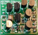
The last modules by Forssell looked like this. I can count more than 7 transistors..
EDIT: Found some more info
"The JFET990-2 uses 8 large source geometry JFET transistors and one NPN transistor (for DC control). Unlike our first generation design the JFET990-2 is differential throughout. It has the standard opamp topology's differential input ports and a single output port. Techniques are used within the JFET990-2 to reduce the input capacitance, however no cascode amplifiers are used. The result is an amplifier with a very simple signal path that has wide bandwidth (-3 dB at >2 megahertz), high slew rate > 60 V/us, and fast rise time (150 nanoseconds)"
P.S. It probably still leaks at +/-24 Volts
Schematic on Forssell's site has this comment:
"First Generation design... that means it is not our latest design"
The last modules by Forssell looked like this. I can count more than 7 transistors..
EDIT: Found some more info
"The JFET990-2 uses 8 large source geometry JFET transistors and one NPN transistor (for DC control). Unlike our first generation design the JFET990-2 is differential throughout. It has the standard opamp topology's differential input ports and a single output port. Techniques are used within the JFET990-2 to reduce the input capacitance, however no cascode amplifiers are used. The result is an amplifier with a very simple signal path that has wide bandwidth (-3 dB at >2 megahertz), high slew rate > 60 V/us, and fast rise time (150 nanoseconds)"
P.S. It probably still leaks at +/-24 Volts
Attachments
Last edited:
Well it appears that there are no future questions about the original Vendetta Research SCP-1. This basic circuit is still viable, but we have moved on in other areas. It must be underlined that this circuit is not 'idiot-proof' like so many IC's. It WILL pick up power supply noise, transients, and hum. Special, low noise buffers must be made to go with them, AND they become part of the circuit's sound, so be careful.
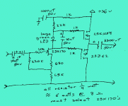
This latest design with 3 fets, 1 jfet and 2 mosfets, is OK, barely. It is simple, almost crude, BUT it should work, and perhaps sound pretty good.
What controls the current through the mosfets? Does this rely on Vth being correct and not drifting with temperature?
Well it appears that there are no future questions about the original Vendetta Research SCP-1. This basic circuit is still viable, but we have moved on in other areas. It must be underlined that this circuit is not 'idiot-proof' like so many IC's. It WILL pick up power supply noise, transients, and hum. Special, low noise buffers must be made to go with them, AND they become part of the circuit's sound, so be careful.
Look at #44028
- Status
- Not open for further replies.
- Home
- Member Areas
- The Lounge
- John Curl's Blowtorch preamplifier part II