TDA1541
Hi Zsolt
+15V it is necessary for TDA1541 2mA offset compensation by schematics in Setup TDA1541A DAC, but -15V,GND (analog, for TDA1541A only) is not needed :
:
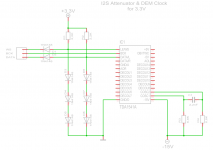
Power connectors for TDA1541: 4x2pin 2.5mm (JST EH series)
+Va, GND (analog) +15V (nulling 2mA offset circuitry)
-Va, GND (analog) -15V (-VDD2, pin 15)
+5V, GND (digital) +5V (VDD, pin 28)
-5V, GND (digital) -5V (-VDD1, pin 26)
Yes, schematics are impressive and really fine.
Solution of 14 SMD 1206 size decoupling capacitors is simple and perfect, as ordered")
I guess one TDA1541 (two PCM channels) should fit on 80x60mm board.
Because original board rev 0003 is about 90x90mm, however almost one quarter of it is free of components and, as you wrote, we do not need a lot of things here.
If we still would have not enough space on 80x60mm board, I would leave off-board DEM clocking circuitry too.
But leaving two options for DEM here: textbook capacitor or external DEM clocking through U.FL connector.
This would also eliminate issue of power supply connector for DEM clocking.
Thanks
Saulius
Regarding connectors, JST has a compact EH 2.5mm pitch series that allows up to AWG22 - for over design aficionados - we can use that.
To sum up what we have so far:
Power connectors: 5x2pin 2.5mm (JST EH series)
+Va, GND (analog)
-Va, GND (analog)
-15V,GND (analog, for TDA1541A only)
+5V, GND (digital)
-5V, GND (digital)
Hi Zsolt
+15V it is necessary for TDA1541 2mA offset compensation by schematics in Setup TDA1541A DAC, but -15V,GND (analog, for TDA1541A only) is not needed
:Power connectors for TDA1541: 4x2pin 2.5mm (JST EH series)
+Va, GND (analog) +15V (nulling 2mA offset circuitry)
-Va, GND (analog) -15V (-VDD2, pin 15)
+5V, GND (digital) +5V (VDD, pin 28)
-5V, GND (digital) -5V (-VDD1, pin 26)
- TDA1541A - 1x - 2 PCM channels. This one needs many additional components so most probably only one will fit. I think the best design I've seen so far is this: Setup TDA1541A DAC. We can take ideas regarding many TDA1541A related features
- PCM1704 - 4x - 4 PCM channels
...
Ian, when you have time please have a look at this: TDA1541A schematics. We don't need from here the PSU part and the 74HC175 reclocking but seems that DEM clocking needs a master clock (MCLKI) input. Do you think one of this beast will fit on an 80x60mm board?
Regards,
Zsolt
Yes, schematics are impressive and really fine.
Solution of 14 SMD 1206 size decoupling capacitors is simple and perfect, as ordered
I guess one TDA1541 (two PCM channels) should fit on 80x60mm board.
Because original board rev 0003 is about 90x90mm, however almost one quarter of it is free of components and, as you wrote, we do not need a lot of things here
. If we still would have not enough space on 80x60mm board, I would leave off-board DEM clocking circuitry too.
But leaving two options for DEM here: textbook capacitor or external DEM clocking through U.FL connector.
This would also eliminate issue of power supply connector for DEM clocking.
Thanks
Saulius
Last edited:
TDA1541
BTW. there are similar offset compensation circuits that work with +5V as well (e.g. OPA861 AYA II DAC). When implementing TDA1541 design will decide which to choose so +Va will be defined accordingly.
Supply of DEM clocking can be +5V (digital) with good filtering as Setup did - no need for special connector for this.
Thanks,
Zsolt
You are correct... distinct -15V,GND (analog, for TDA1541A only) is not needed because it will be supplied at -Va.+15V it is necessary for TDA1541 2mA offset compensation by schematics in Setup TDA1541A DAC, but -15V,GND (analog, for TDA1541A only) is not needed
Power connectors for TDA1541: 4x2pin 2.5mm (JST EH series)
+Va, GND (analog) +15V (nulling 2mA offset circuitry)
-Va, GND (analog) -15V (-VDD2, pin 15)
+5V, GND (digital) +5V (VDD, pin 28)
-5V, GND (digital) -5V (-VDD1, pin 26)
BTW. there are similar offset compensation circuits that work with +5V as well (e.g. OPA861 AYA II DAC). When implementing TDA1541 design will decide which to choose so +Va will be defined accordingly.
I think both should be included but DEM clocking definitely.But leaving two options for DEM here: textbook capacitor or external DEM clocking through U.FL connector.
This would also eliminate issue of power supply connector for DEM clocking
Supply of DEM clocking can be +5V (digital) with good filtering as Setup did - no need for special connector for this.
Thanks,
Zsolt
TDA1541
Maybe I'm wrong, but it looks like digital attenuators in TDA1541A schematics are for 5V, not for 3.3V signals.
I2S-PCM board output signals are 3.3V.
Ian, when you have time please have a look at this: TDA1541A schematics.
Maybe I'm wrong, but it looks like digital attenuators in TDA1541A schematics are for 5V, not for 3.3V signals.
I2S-PCM board output signals are 3.3V.
Again, the TDA1541A is a totally different DAC and need a different approach (DEM, I2S attenuation, offset nulling since it swings from 0 to -4mA and more), and IMHO board size cannot be a limit. For example SMD caps seem are not the best solution for DEM.
Please, take a look at John thread located at
http://www.diyaudio.com/forums/digi...building-ultimate-nos-dac-using-tda1541a.html
Please, take a look at John thread located at
http://www.diyaudio.com/forums/digi...building-ultimate-nos-dac-using-tda1541a.html
We want to standardize the power connectors position and type - that's it.I don't understand why you try to standardize power connector if every core board will be supplied with different external PSUs..
Why? because ideally these nice PCBs should end up in a case - most probably tightly fit among lot of low noise regulators, I2S source, I/V and who knows what else... that's OK unless at some point you want to try out another DAC. I'm sure many of us want to do that... so this standardization will make life easier for those who want to experiment.
Why cannot you use the same external PSU with AD1865 and AD1862? switch boards, configure your PSU for +/-12V and you are ready to roll.
TDA1541
There are #4955 posts. Please refer to those that talk about DEM caps or I2S attenuation.Again, the TDA1541A is a totally different DAC and need a different approach (DEM, I2S attenuation, offset nulling since it swings from 0 to -4mA and more), and IMHO board size cannot be a limit. For example SMD caps seem are not the best solution for DEM.
Please, take a look at John thread located at
http://www.diyaudio.com/forums/digi...building-ultimate-nos-dac-using-tda1541a.html
TDA1541
Would you like to research the I2S-PCM - TDA1541 core board related stuff? E.g. filtering/level matching of DEM/I2S lines (level matching might not be needed), DEM clocking... etc.
Thanks,
Zsolt
I know nothing about these TDA1541 specific features that's why I searched for a seemingly well and carefully designed project.Maybe I'm wrong, but it looks like digital attenuators in TDA1541A schematics are for 5V, not for 3.3V signals.
I2S-PCM board output signals are 3.3V.
Would you like to research the I2S-PCM - TDA1541 core board related stuff? E.g. filtering/level matching of DEM/I2S lines (level matching might not be needed), DEM clocking... etc.
Thanks,
Zsolt
Last edited:
There are #4955 posts. Please refer to those that talk about DEM caps or I2S attenuation.
Several people tried to get best performance from TDA1541A and spent years to reach optimal results (John is one of those), so is not a simple project, and surely cannot be solved in a few posts on this thread.
I think firstly we have to decide if we want build one of the many anonymous circuits, or we want follow the tips of those who have experimented along years, or even we want start a new research to get the best performance.
Next days I'll try to extract the most significant posts from John's thread, but I think there is nothing to standardize about TDA1541A, it's too different from the other DAC chips
TDA1541
Thanks,
Zsolt
I think we want to "follow the tips of those who have experimented along years" so it would be really useful if you could gather/extract these from sources you best know (John's thread or other).I think firstly we have to decide if we want build one of the many anonymous circuits, or we want follow the tips of those who have experimented along years, or even we want start a new research to get the best performance.
Next days I'll try to extract the most significant posts from John's thread, but I think there is nothing to standardize about TDA1541A, it's too different from the other DAC chips
Thanks,
Zsolt
TDA1541
And you found right project, we simply need to remove something, that is less needed in your Core Board project.
I already wrote my suggestion what is necessary to leave "onboard" in post#41.
Concerning 3.3V attenuators - I'm not sure those are needed at all, because "bouncing effect" is most sensible with 5V levels.
Yes, I would like it.
I'm sure we are not going to make new research.
We are not going to search unending "ultimate" solution, because this "ultimate" is like unreachable Utopia, it evolves during your study, like time/position issue with elementary particles in quantum physics
We need take for this moment best proven ideas from community and place it on Core Board, preferably 80x60mm or 80x70mm.
Fine, we appreciate your help.
But I disagree about TDA1541 "is too different from the other DAC chip".
It still has powers supply, inputs and outputs.
And we are going to make Core Board, not a new DAC chip
We can and need to "standardize" inputs and outputs of core board:
1. power supply sockets;
2. inputs of data in simultaneous mode (placing compatible sockets in dedicated places, aligned with I2S-PCM outputs );
3. analog outputs - preferably to have null offset current;
Those are basic requirements.
All the other solutions (attenuators for incoming signals, pin and/or SMD type decoupling and DEM capacitors, inputs for external DEM clock or local DEM clocking circuit driven by BCK, or free DEM clocking proposed by John, type of 2mA injecting circuitry, etc) should be suggested and discussed and placed "onboard" if there still be enough place.
Saulius
I know nothing about these TDA1541 specific features that's why I searched for a seemingly well and carefully designed project.
And you found right project, we simply need to remove something, that is less needed in your Core Board project.
I already wrote my suggestion what is necessary to leave "onboard" in post#41.
Concerning 3.3V attenuators - I'm not sure those are needed at all, because "bouncing effect" is most sensible with 5V levels.
Would you like to research the I2S-PCM - TDA1541 core board related stuff? E.g. filtering/level matching of DEM/I2S lines (level matching might not be needed), DEM clocking... etc.
Yes, I would like it.
I think firstly we have to decide if we want build one of the many anonymous circuits, or we want follow the tips of those who have experimented along years, or even we want start a new research to get the best performance.
I'm sure we are not going to make new research.
We are not going to search unending "ultimate" solution, because this "ultimate" is like unreachable Utopia, it evolves during your study, like time/position issue with elementary particles in quantum physics
We need take for this moment best proven ideas from community and place it on Core Board, preferably 80x60mm or 80x70mm.
Next days I'll try to extract the most significant posts from John's thread, but I think there is nothing to standardize about TDA1541A, it's too different from the other DAC chips
Fine, we appreciate your help.
But I disagree about TDA1541 "is too different from the other DAC chip".
It still has powers supply, inputs and outputs.
And we are going to make Core Board, not a new DAC chip
We can and need to "standardize" inputs and outputs of core board:
1. power supply sockets;
2. inputs of data in simultaneous mode (placing compatible sockets in dedicated places, aligned with I2S-PCM outputs );
3. analog outputs - preferably to have null offset current;
Those are basic requirements.
All the other solutions (attenuators for incoming signals, pin and/or SMD type decoupling and DEM capacitors, inputs for external DEM clock or local DEM clocking circuit driven by BCK, or free DEM clocking proposed by John, type of 2mA injecting circuitry, etc) should be suggested and discussed and placed "onboard" if there still be enough place.
Saulius
Question of point of view: I think your idea about TDA1541A is completely wrong, and you are thinking to an unuseful board with that DAC chip, but again this is my subjective opinion.
vzs,
for the moment I'm just remembering then I'll list some useful links.
- DEM clock: someone likes free running DEM, some other prefer sync DEM, so we could provide both option. Most people claim that a relatively low DEM frequency is better, around 88 kHz, so the board should accomodate a simple capacitor between OSC pin, a styrene cap is preferable, so a through hole component (around 1nF for 88 kHz). For sync option we could provide the place for an external clock and maybe a frequency multiplier on board starting from WS signal (2x).
- if the board will provide the place for a IV resistor, this should be through hole to accomodate a metal foil or wirewound resistor (good results have been reached with Vishay Z-Foil or Rhopoint Econistor).
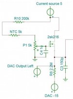
- the board should provide a CCS to nulling the offset caused by the current output characteristic of the TDA1541A (from 0 to -4 mA). Also, this offset circuit should have very low drift. Somehing similar to the circuit used from Oliver in his Red Baron should be ok, adding an NTC.
- since TDA1541A shouldn't swing more than +/- 25 mV to avoid distorsion, the IV resistor have to be very low (10-12 ohm), with serious problem of S/N, one could think to an easy paralleling DAC board, to accomodate 4 or more DAC chips, to use an higher IV resistor value
- for the I2S attenuation i'll post the link to John's solution
- about decoupling capacitor, seems best results are reached with MKP capacitor, such Wima or Siemens, so through hole place for them, but since someone prefer SMD caps the board could provide both option (one at component side, the other at bottom side)
TDA1541
Of course it is question of point of view: I wrote only my opinion about primary requirements (as base) which should be fulfilled about core board.
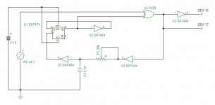
I prefer free running DEM, but with possibility to connect external clock. Look into attachment for Olivier's (with help by John) schematic for free running DEM clock as well as 3.3V version of I2S attenuator.
We can use same attenuation circuitry for DATA/L and DATA/R, BCK and LE do not need attenuation. Problem here can be 3.3V clean source.
Primary idea of core board was to leave everything about I/U conversion outside the board, except maybe 2mA injector, including all worries about S/N.
Anyway, thank you Oliver for finding Rhopoint Econistor
If you mean excellent MK7 type reclock with D flip flops without passive attenuation, I have attached that schematics here, but I doubt we would use such a complicated circuitry for debouncing in core board...Link is here - http://www.diyaudio.com/forums/digital-line-level/79452-building-ultimate-nos-dac-using-tda1541a-366.html#post2549175
I would vote for 1206 size capacitors SMD type, like in schematics provided by Zsolt: Setup TDA1541A DAC, on the bottom side under TDA1541.
If someones wants pin type solution please ask Oliver - he has enough of Red Baron.
Really I like Red Baron and everything is ok with ones, I have myself few boards installed and few unused - soldered and ready to use, and was ready to go for RB V5.0 but Zsolt wrote something about CORE BOARD and I think it is worth to try.
Because I have small problem with my project- all version of Red Baron is simply to long for my unending "ultimate" project... If it would be shorter by 40 - 45 mm...
And I would vote not for MKP decoupling on DEM (shadows of Lukasz Fikus ), but for better COG/NPO, only later MKP, X7R, Acrylic FPA or at least MKT stacked structure (lowest ESL). Do not use any electrolytic here - I have tried tantalum SMD, Silmics, Oscons and Black Gates NX (favorites of famous Pedja Rogic), but simple X7R sound far better...
And I'm not sure polystyrene capacitors are best choice for free running DEM - I saw 1% silver mica as well as even more NPO capacitors on pins 16.17...
Best wishes
Saulius
Question of point of view: I think your idea about TDA1541A is completely wrong, and you are thinking to an unuseful board with that DAC chip, but again this is my subjective opinion.
Of course it is question of point of view: I wrote only my opinion about primary requirements (as base) which should be fulfilled about core board. vzs,
for the moment I'm just remembering then I'll list some useful links.
- DEM clock: someone likes free running DEM, some other prefer sync DEM, so we could provide both option.
I prefer free running DEM, but with possibility to connect external clock. Look into attachment for Olivier's (with help by John) schematic for free running DEM clock as well as 3.3V version of I2S attenuator.
We can use same attenuation circuitry for DATA/L and DATA/R, BCK and LE do not need attenuation. Problem here can be 3.3V clean source.
- if the board will provide the place for a IV resistor, this should be through hole to accomodate a metal foil or wirewound resistor (good results have been reached with Vishay Z-Foil or Rhopoint Econistor).
- the board should provide a CCS to nulling the offset caused by the current output characteristic of the TDA1541A (from 0 to -4 mA). Also, this offset circuit should have very low drift. Somehing similar to the circuit used from Oliver in his Red Baron should be ok, adding an NTC.
- since TDA1541A shouldn't swing more than +/- 25 mV to avoid distorsion, the IV resistor have to be very low (10-12 ohm), with serious problem of S/N, one could think to an easy paralleling DAC board, to accomodate 4 or more DAC chips, to use an higher IV resistor value
Primary idea of core board was to leave everything about I/U conversion outside the board, except maybe 2mA injector, including all worries about S/N.
Anyway, thank you Oliver for finding Rhopoint Econistor
- for the I2S attenuation i'll post the link to John's solution
If you mean excellent MK7 type reclock with D flip flops without passive attenuation, I have attached that schematics here, but I doubt we would use such a complicated circuitry for debouncing in core board...Link is here - http://www.diyaudio.com/forums/digital-line-level/79452-building-ultimate-nos-dac-using-tda1541a-366.html#post2549175
- about decoupling capacitor, seems best results are reached with MKP capacitor, such Wima or Siemens, so through hole place for them, but since someone prefer SMD caps the board could provide both option (one at component side, the other at bottom side)
I would vote for 1206 size capacitors SMD type, like in schematics provided by Zsolt: Setup TDA1541A DAC, on the bottom side under TDA1541.
If someones wants pin type solution please ask Oliver - he has enough of Red Baron.
Really I like Red Baron and everything is ok with ones, I have myself few boards installed and few unused - soldered and ready to use, and was ready to go for RB V5.0 but Zsolt wrote something about CORE BOARD and I think it is worth to try.
Because I have small problem with my project- all version of Red Baron is simply to long for my unending "ultimate" project...
If it would be shorter by 40 - 45 mm...And I would vote not for MKP decoupling on DEM (shadows of Lukasz Fikus
), but for better COG/NPO, only later MKP, X7R, Acrylic FPA or at least MKT stacked structure (lowest ESL). Do not use any electrolytic here - I have tried tantalum SMD, Silmics, Oscons and Black Gates NX (favorites of famous Pedja Rogic), but simple X7R sound far better...And I'm not sure polystyrene capacitors are best choice for free running DEM - I saw 1% silver mica as well as even more NPO capacitors on pins 16.17...
Best wishes
Saulius
Attachments
Last edited:
Well...
- free running DEM clock: I don't know any reason to avoid styrene caps, but let me learn... the simplest way is to provide both options, through hole footprint at top side level for styrene or silver mica and SMD footprint at top side for X7R or so
- sync DEM: we could provide this option, as an alternative, simple pads for external clock or maybe a synchronous clock starting from WS signal by fequency multiplier (simple schematic attached)
- IV resistor: since many of us (I think) will use a simple resistor as I to V converter, followed by a gain/buffer stage, I think the board should provide the footprint inside it for all DAC chip. I don't see any reason to keep the IV resistor external, with long wires and problem related, simply the core board should provide the footprint for that resistor, Vishay Z-Foil, Econistor or SMD at bottom side level for SMD lovers
- I2S attenuation: noizas has just provided the schematic, I subscribe that way
- offset nulling: we could use part of Red Baron schematic, with 2SK216, removing the IV resistor and adding an NTC in series with the trimmer (I attach a schematic, courtesy of Ryanj). The 150pF capacitor at the output limits the bandwidth.
- paralleling: as well known the TDA1541A shouldn't swing more than +/- 25mV when loaded with IV resistor to avoid distorsion, a very very low output level compared to the voltage coming from other DAC chip. For example the AD1865 can drive easily a 220R resistor to provide hundreds of mV at its output (I own a similar DAC and it sounds pretty good). So an easy paralleleng of the TDA should be the right way to increase the output voltage level, similar to other DAC chips. Not very simple to implement, but I think we should investigate this option
- decoupling caps: please take a look at Jameshillj experience http://www.diyaudio.com/forums/digi...ding-ultimate-nos-dac-using-tda1541a-491.html #4907. Again, I think the board should provide both options, through hole footprint at top side and 1206 footprint at bottom side for SMD lovers. It's not so difficult to provide both options.
Finally...
I think we would worry about the performance rather than the board size, but if all member who joined this thread are worried about dimensional features, this is the wrong thread for me, and I give up and I leave it immediately.
Again, the TDA1541A DAC chip is totally different from the other DAC. In my AD1865 DAC there are a few components (DAC chip, one 74HC04 and a few decoupling capacitors), but the TDA1541A is another story.
Attachments
P.S.
The TDA1541A is naturally I2S compliant, so it doesn't need any I2S to PCM conversion, the FIFO buffer can feed it directly (better without the reclock board, but this is another story).
And rather than dual mono option, for all DAC chip, I would think about a balanced option, for example to feed directly a 6H30 circlotron output stage.
TDA1541
I subscribe for all above - it is all reasonable, main ideas are tested by many DIYers and flexible options are welcome.
I wouldn't be so enthusiastic about paralleling of outputs "to increase output voltage level". It is suitable for decreasing DA errors and possibly to increase dynamic range, but not to have "gain".
Shortly, paralleling of two outputs means increasing of current swing twice - from 0 to -8mA, so it should lead to decreasing I/U resistor twice (Ohm law) simply to have same ±25 mV range on parallel outputs.
Because it is the same output (outputs) with applied voltage, does not matter is it loaded by I/U resistor or OPAMP I/U circuitry or primary coil of audio transformer, voltage on it should be within ±25 mV range (to AGND).
But this is possibly off topic here - if someones need paralleling, can do it simply paralleling core boards.
Andrea, what do you want to add on core board for paralleling - some special connector for stacking boards on each other or something else? Please explain.
About through hole capacitors for DEM decoupling - this should be an option if we still have space on core board for them.
Please look for John's players - all latest of them are with SMD DEM decoupling capacitors, as well as last two version of Red Barons.
I also would be glad to make more experiments with those through hole capacitors on core board, but I also can do such experiments on Red Baron...
I agree that TDA1541 is another story, but this does not mean we should leave possibilty to make TDA1541 core board compatible with I2S-PCM/FIFO or FIFO+Clock board in size and outputs/intputs digital connectors...
You are completely right, but there it is an idea to make four PCM channel solution (as it is after I2S-PCM board), allowing balanced operation.
For really balanced operation in I2S mode you need have two I2S streams with normal and inverted data for left and right channel separately.
For that you can use circuitry of Pedja Rogic (I have attached it), as I have intended before I2S-PCM era and actually already have all components ready.
Unfortunately, it is very limited in speed because of shift register HEF4517.
Even with special way of powering HEF4517 and level matching on inputs and outputs I doubt you can achieve more than 48kHz sampling rate...
It is completely up to you.
With I2S-PCM board and two TDA1541 core board (two PCM channel per board) you would have possibility to make whatever you want:
1. 4x paralleled mono;
2. 2x paralleled stereo;
3. 1x fully balanced stereo.
I'm making fully balanced stereo in my DAC project, so I would be glad to have all FIFO+PCM+core board solution.
As I/U conversion I will use Rhopoint Econistor +Sowter 9545z or LL7903 to have in one shot:
filtering HF, eliminating DA conversion errors (as it will be balanced in one TDA1541), and a little bit gain.
Regards
Saulius
Well...
- free running DEM clock: I don't know any reason to avoid styrene caps, but let me learn... the simplest way is to provide both options, through hole footprint at top side level for styrene or silver mica and SMD footprint at top side for X7R or so
- sync DEM: we could provide this option, as an alternative, simple pads for external clock or maybe a synchronous clock starting from WS signal by fequency multiplier (simple schematic attached)
- IV resistor: since many of us (I think) will use a simple resistor as I to V converter, followed by a gain/buffer stage, I think the board should provide the footprint inside it for all DAC chip. I don't see any reason to keep the IV resistor external, with long wires and problem related, simply the core board should provide the footprint for that resistor, Vishay Z-Foil, Econistor or SMD at bottom side level for SMD lovers
- I2S attenuation: noizas has just provided the schematic, I subscribe that way
- offset nulling: we could use part of Red Baron schematic, with 2SK216, removing the IV resistor and adding an NTC in series with the trimmer (I attach a schematic, courtesy of Ryanj). The 150pF capacitor at the output limits the bandwidth.
I subscribe for all above - it is all reasonable, main ideas are tested by many DIYers and flexible options are welcome.
- paralleling: as well known the TDA1541A shouldn't swing more than +/- 25mV when loaded with IV resistor to avoid distorsion, a very very low output level compared to the voltage coming from other DAC chip. For example the AD1865 can drive easily a 220R resistor to provide hundreds of mV at its output (I own a similar DAC and it sounds pretty good). So an easy paralleleng of the TDA should be the right way to increase the output voltage level, similar to other DAC chips. Not very simple to implement, but I think we should investigate this option
I wouldn't be so enthusiastic about paralleling of outputs "to increase output voltage level". It is suitable for decreasing DA errors and possibly to increase dynamic range, but not to have "gain".
Shortly, paralleling of two outputs means increasing of current swing twice - from 0 to -8mA, so it should lead to decreasing I/U resistor twice (Ohm law) simply to have same ±25 mV range on parallel outputs
.Because it is the same output (outputs) with applied voltage, does not matter is it loaded by I/U resistor or OPAMP I/U circuitry or primary coil of audio transformer, voltage on it should be within ±25 mV range (to AGND).
But this is possibly off topic here - if someones need paralleling, can do it simply paralleling core boards.
Andrea, what do you want to add on core board for paralleling - some special connector for stacking boards on each other or something else? Please explain.
- decoupling caps: please take a look at Jameshillj experience http://www.diyaudio.com/forums/digi...ding-ultimate-nos-dac-using-tda1541a-491.html #4907. Again, I think the board should provide both options, through hole footprint at top side and 1206 footprint at bottom side for SMD lovers. It's not so difficult to provide both options.
About through hole capacitors for DEM decoupling - this should be an option if we still have space on core board for them.
Please look for John's players - all latest of them are with SMD DEM decoupling capacitors, as well as last two version of Red Barons.
I also would be glad to make more experiments with those through hole capacitors on core board, but I also can do such experiments on Red Baron...
Finally...
I think we would worry about the performance rather than the board size, but if all member who joined this thread are worried about dimensional features, this is the wrong thread for me, and I give up and I leave it immediately.
Again, the TDA1541A DAC chip is totally different from the other DAC. In my AD1865 DAC there are a few components (DAC chip, one 74HC04 and a few decoupling capacitors), but the TDA1541A is another story.
I agree that TDA1541 is another story, but this does not mean we should leave possibilty to make TDA1541 core board compatible with I2S-PCM/FIFO or FIFO+Clock board in size and outputs/intputs digital connectors...
P.S.
The TDA1541A is naturally I2S compliant, so it doesn't need any I2S to PCM conversion, the FIFO buffer can feed it directly (better without the reclock board, but this is another story).
You are completely right, but there it is an idea to make four PCM channel solution (as it is after I2S-PCM board), allowing balanced operation.
For really balanced operation in I2S mode you need have two I2S streams with normal and inverted data for left and right channel separately.
For that you can use circuitry of Pedja Rogic (I have attached it), as I have intended before I2S-PCM era
and actually already have all components ready.Unfortunately, it is very limited in speed because of shift register HEF4517.
Even with special way of powering HEF4517 and level matching on inputs and outputs I doubt you can achieve more than 48kHz sampling rate...
And rather than dual mono option, for all DAC chip, I would think about a balanced option, for example to feed directly a 6H30 circlotron output stage.
It is completely up to you.
With I2S-PCM board and two TDA1541 core board (two PCM channel per board) you would have possibility to make whatever you want
:1. 4x paralleled mono;
2. 2x paralleled stereo;
3. 1x fully balanced stereo.
I'm making fully balanced stereo in my DAC project, so I would be glad to have all FIFO+PCM+core board solution.
As I/U conversion I will use Rhopoint Econistor +Sowter 9545z or LL7903 to have in one shot:
filtering HF, eliminating DA conversion errors (as it will be balanced in one TDA1541), and a little bit gain
.Regards
Saulius
Attachments
Last edited:
You are right, to increase the output voltage the TDAs should be in series, not paralleling.
About "easy paralleling" I mean the DAC chip could share all except for the DEM circuit, so I mean suitable pins to "quasi piggy" the chips.
For balanced mode, of course, the I2S to PCM board is wellcome, but for unbalanced mode I wouldn't use it, simply to not add more jitter coming from another stage.
About the clock (and jitter), I would feed directly the DAC at 128fs (5.6448MHz) and then send it back to the FIFO board without reclock section, but this is off topic in this thread.
TDA1541
Thank you guys for extracting information about open questions.
Summarizing:
- All core boards are thought to be used after I2S-PCM board only, _no I2S input_: dvb projekt comment about I2S input when testing I2S-PCM with his Red Baron v5.0: "i will never go back to the I2S input!"
- free running DEM clock: support for both SMD (1206) and thorough-hole (5mm ?) footprints
- sync DEM: master clock U-FL input needed only for this DAC
- IV resistor: since many are using these DACs with passive I/V (resistor || capacitor) and require low board space I think we should add this
- I2S attenuation: schematics attached by noizas in #53 - will need to recalculate the 2.2K resistors for 5V supply
- offset nulling: Pedja's Aya DAC shows a simple solution around a low noise JFet
- decoupling: SMD caps only (Successful PCB grounding with mixed-signal chips - Part 2: Design to minimize signal-path crosstalk | EDN)
- paralleling: only dual-mono configuration through provided U-FL connectors. Piggybacking ICs or core boards (e.g. with pin headers/connectors) will not be provided due to signal integrity concerns
- size: with most of your suggestions it should probably fit on a "standard" size core board - don't know exact size yet but will target 80x60mm
Thanks,
Zsolt
TDA1541
Excellent summary
1. About free running DEM clock through hole capacitor:
most of polystyrene in range 470pF - 2nF are 3-8 mm in diameter, as usual about 10mm lenght (depends on voltage). So it would be better to have at least 7.5 footprint.
2. About I/V resistor - I would make two sets of footprint - for axial and for compact size (MK132).
3. LVTTL attenuation with 5V instead of 3.3V: I see no need to increase 2K2 resistors, because signal swing anyway will be between 0.6V and 1.8V (diodes), just current through 2K2 will be increased by 0.8mA.
Change 2K2 to higher value would lead to worse slew rate on inputs of TDA1541 (increased RC value).
However this suggestion simply replace 3.3V by 5V source should be checked by Ian - I do not know I2S-PCM board's output capability to sink such additional 0.8mA current (actually almost 2mA instead of 1.2mA).
Thanks
Saulius
Thank you guys for extracting information about open questions.
Summarizing:
- All core boards are thought to be used after I2S-PCM board only, _no I2S input_: dvb projekt comment about I2S input when testing I2S-PCM with his Red Baron v5.0: "i will never go back to the I2S input!"
- free running DEM clock: support for both SMD (1206) and thorough-hole (5mm ?) footprints
- sync DEM: master clock U-FL input needed only for this DAC
- IV resistor: since many are using these DACs with passive I/V (resistor || capacitor) and require low board space I think we should add this
- I2S attenuation: schematics attached by noizas in #53 - will need to recalculate the 2.2K resistors for 5V supply
- offset nulling: Pedja's Aya DAC shows a simple solution around a low noise JFet
- decoupling: SMD caps only (Successful PCB grounding with mixed-signal chips - Part 2: Design to minimize signal-path crosstalk | EDN)
- paralleling: only dual-mono configuration through provided U-FL connectors. Piggybacking ICs or core boards (e.g. with pin headers/connectors) will not be provided due to signal integrity concerns
- size: with most of your suggestions it should probably fit on a "standard" size core board - don't know exact size yet but will target 80x60mm
Thanks,
Zsolt
Excellent summary
1. About free running DEM clock through hole capacitor:
most of polystyrene in range 470pF - 2nF are 3-8 mm in diameter, as usual about 10mm lenght (depends on voltage). So it would be better to have at least 7.5 footprint.
2. About I/V resistor - I would make two sets of footprint - for axial and for compact size (MK132).
3. LVTTL
attenuation with 5V instead of 3.3V: I see no need to increase 2K2 resistors, because signal swing anyway will be between 0.6V and 1.8V (diodes), just current through 2K2 will be increased by 0.8mA. Change 2K2 to higher value would lead to worse slew rate on inputs of TDA1541 (increased RC value).
However this suggestion simply replace 3.3V by 5V source should be checked by Ian - I do not know I2S-PCM board's output capability to sink such additional 0.8mA current (actually almost 2mA instead of 1.2mA).
Thanks
Saulius
TDA1541
One aspect regarding TDA1541 core board was not decided: synchronous DEM clocking
I'm not sure we should follow Setup's design as there are many different DEM clocking circuits floating around... from ones like Henk Ten Pierick’s to others using a simple inverter on BCK. Also this thread discusses TDA1541 DEM reclocking but I'm sure -ecdesigns- marathon thread has lot of information.
Which implementation should we use?
What about having free running DEM clock only on the core board and have synchronous DEM clocking on a daughter board - e.g. simply plugged into an 14pin IC header or similar - one could try different implementations like that. Nevertheless we should implement one of the synchronous DEM clocking solutions on this daughter board.
Thanks,
Zsolt
- Status
- This old topic is closed. If you want to reopen this topic, contact a moderator using the "Report Post" button.
- Home
- Source & Line
- Digital Line Level
- Multibit DAC core boards coupled with I2S-PCM driver board