gtG ucd ver 2.1
hi all my ucd version 2.0 worked well with very high power and effeciency because i used +/-67 vlts and irf640n x 3pairs with a 4 ohm kenwood 3010 woofer . i pushed the amp hard for about 5 min and the fets did not even warm and they were not mounted on any heatsink. i did not continue with driving the amp hard because the power was too much i feared destroying the woofer.
 the disadvantages of my amp were obvious .
>>>the noise hf, (as lorylaci pointed out ) was too much a nuisance that it is heard even in a subwoofer so my poor lay out cannot be used as a subwoofer amp <<<
>>> i disconnected the protection circuit at ir2110 sd pin 11 because it was always turning on even at medium volumes and the relay part was not working at all and the output without load was measuring that it had dc., but when i connected load all was o.k except noise <<<
>>>the output core ei33 with 14 turns single 0.8mm wire . the wires were extremely hot . mine guess is that they could not survive 30 mins in real world applications <<<
advantages
>>> i like this ucd amp laszlo (lorylaci)version because of the precise and simple frequency controll. once i changed from using 220pf and i used 1nf the fets were cool and worked o.k " i did not hear a change in sound quality as i lowered the sw freq , maybe the hf noise affected my judgement "<<<
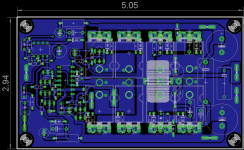
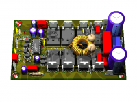
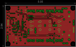
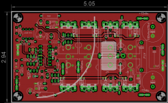
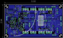
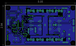
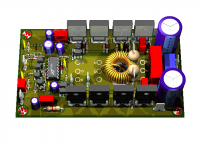
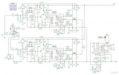
i have done a version 2.1. i hope the layout is o.k . i have taken many precautions including shortening the path of the gate drivers.
i have removed the aux 12 side .the 12vlts aux fet was producing much heat it is better to use an external 12volts stable power supply.
also i did not include the protection board i will make an extra board once laszlo posts his schematic.
any comments and ideas would be helpful . because i want to etch the board
hi all my ucd version 2.0 worked well with very high power and effeciency because i used +/-67 vlts and irf640n x 3pairs with a 4 ohm kenwood 3010 woofer . i pushed the amp hard for about 5 min and the fets did not even warm and they were not mounted on any heatsink. i did not continue with driving the amp hard because the power was too much i feared destroying the woofer.
the disadvantages of my amp were obvious . >>>the noise hf, (as lorylaci pointed out ) was too much a nuisance that it is heard even in a subwoofer so my poor lay out cannot be used as a subwoofer amp
<<< >>> i disconnected the protection circuit at ir2110 sd pin 11 because it was always turning on even at medium volumes and the relay part was not working at all and the output without load was measuring that it had dc., but when i connected load all was o.k except noise <<<
>>>the output core ei33 with 14 turns single 0.8mm wire . the wires were extremely hot . mine guess is that they could not survive 30 mins in real world applications <<<
advantages
>>> i like this ucd amp laszlo (lorylaci)version because of the precise and simple frequency controll. once i changed from using 220pf and i used 1nf the fets were cool and worked o.k " i did not hear a change in sound quality as i lowered the sw freq , maybe the hf noise affected my judgement "<<<
i have done a version 2.1. i hope the layout is o.k . i have taken many precautions including shortening the path of the gate drivers.
i have removed the aux 12 side .the 12vlts aux fet was producing much heat it is better to use an external 12volts stable power supply.
also i did not include the protection board i will make an extra board once laszlo posts his schematic.
any comments and ideas would be helpful . because i want to etch the board
Attachments
-
 gtG ucd 1100 rev 2.1 board bottom.png47.8 KB · Views: 2,714
 -
gtG ucd 1100 rev 2.1 schematic.pdf36.8 KB · Views: 837
-
 gtG ucd 1100 rev 2.1 simulation .png142.8 KB · Views: 1,441
 -
 gtG ucd 1100 rev 2.1 schematic.png121 KB · Views: 1,415
 -
 gtG ucd 1100 rev 2.1 board pcb top.png52.6 KB · Views: 530
 -
 gtG ucd 1100 rev 2.1 board pcb components.png113 KB · Views: 2,313
 -
 gtG ucd 1100 rev 2.1 board pcb components 2.png118.3 KB · Views: 2,422
 -
 gtG ucd 1100 rev 2.1 board pcb bottom.png54.9 KB · Views: 2,530
 -
 gtG ucd 1100 rev 2.1 2.png150.1 KB · Views: 2,652
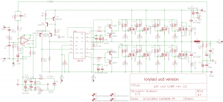
only 1uF for bootstrap electrolytic cap? Or is it an error?
R18 may be 22k
Input pin of LM311 are inverted.
Try to rise the LM311's supply and see what happens to noise.
Remove output snubber R17+C11 . It's an UCD design, so NO snubber on output.
All 10k pull-down gate resistor are useless. One is enough before gate resistors.
Layout is good.
LM311 it's no so good. I use LT1016.
thanks pergo for reply . the inputs are derived from schema from hobbyelectronica.com http://www.hobbielektronika.hu/cikkek/files/808/ucd_ir_hid_k_jav.jpg
http://translate.googleusercontent....l?pg=1&usg=ALkJrhgYKUIIOvlB0-VDtruHr5nh-rRfCg
what lm ic can be used instead of lt1016?
http://translate.googleusercontent....l?pg=1&usg=ALkJrhgYKUIIOvlB0-VDtruHr5nh-rRfCg
what lm ic can be used instead of lt1016?
Attachments
Last edited:
LT1016 offers complementary output and it's easy to use with IR2110
But this schematic has a fixed (and unknown) deadtime.
It works perfectly with fast mosfets like IRF540Z.
Or, if you want to use a simple comparator with only one output, you can use IRS20957 instead IR2110.
Basically it's a IR2010 with single floating input (no level shifter), internal phase splitter, advanced protection and variable deadtime.
The schematic will be simpler.
Anyway.
Can you check the LM311's output at idle? (with oscillation started)
(set o-scope 10x zoom and your probe with 1:10 to unload LM311 from parasitics)
An externally hosted image should be here but it was not working when we last tested it.
But this schematic has a fixed (and unknown) deadtime.
It works perfectly with fast mosfets like IRF540Z.
Or, if you want to use a simple comparator with only one output, you can use IRS20957 instead IR2110.
Basically it's a IR2010 with single floating input (no level shifter), internal phase splitter, advanced protection and variable deadtime.
The schematic will be simpler.
Anyway.
Can you check the LM311's output at idle? (with oscillation started)
(set o-scope 10x zoom and your probe with 1:10 to unload LM311 from parasitics)
Last edited:
>>>the noise hf, (as lorylaci pointed out ) was too much a nuisance that it is heard even in a subwoofer so my poor lay out cannot be used as a subwoofer amp
The layout is STILL not better. It is still alayout of a Class-B amp.
>>> i disconnected the protection circuit at ir2110 sd pin 11 because it was always turning on even at medium volumes and the relay part was not working at all and the output without load was measuring that it had dc., but when i connected load all was o.k except noise <<<
For any appliaction over 100W FORGET RELAY!
A relay that can switch off a current more than 10A to resisitve and 6A to inductive load is very ixpensive. Otherwise you are relying on a false hope.
If you need to disconnect the load use a MOSFET relay. If you want to protect the speaker, use Crowbar protection.
EI33 is useful up to about 500W, for over that, you need bigger core, with proper winding. You should take attention to Eddy current losses (winding over the gap causes it).>>>the output core ei33 with 14 turns single 0.8mm wire . the wires were extremely hot . mine guess is that they could not survive 30 mins in real world applications <<<
Layout is very not okay.i have done a version 2.1. i hope the layout is o.k . i have taken many precautions including shortening the path of the gate drivers.
Again:
- Use SMT gate driver buffers PER FET, right next to each FET gate. (specially for turn OFF)
- think about using full-bridge instead of half bridge. For full bridge: you can use 100V FETs instead of 200V, no bus pumping at all, can use simple portection for low side FETs.
- Use proper RC snubber right next to each FET drain and source. (the capacitor value should be at least half of the FETs Coss, and resistor value shoud be about 2-20 Ohm)
I simulated the gate driver stage of yours: it gives about 300ns rise times and 200ns fall times (100nC gate charge, 2N2222A and 2N2907A driver, 3 FETs, including PCB track parasitics). If you use an SMT driver stage per fat you can cut fall time down to 50ns (and rise time to 100ns), enableing an use of small dead-times like 50ns.
Last edited:
care to share your schematic and board layout so that we could all learn how to properly design a good module?The layout is STILL not better. It is still alayout of a Class-B amp.
For any appliaction over 100W FORGET RELAY!
A relay that can switch off a current more than 10A to resisitve and 6A to inductive load is very ixpensive. Otherwise you are relying on a false hope.
If you need to disconnect the load use a MOSFET relay. If you want to protect the speaker, use Crowbar protection.
EI33 is useful up to about 500W, for over that, you need bigger core, with proper winding. You should take attention to Eddy current losses (winding over the gap causes it).
Layout is very not okay.
Again:
- Use SMT gate driver buffers PER FET, right next to each FET gate. (specially for turn OFF)
- think about using full-bridge instead of half bridge. For full bridge: you can use 100V FETs instead of 200V, no bus pumping at all, can use simple portection for low side FETs.
- Use proper RC snubber right next to each FET drain and source. (the capacitor value should be at least half of the FETs Coss, and resistor value shoud be about 2-20 Ohm)
care to share your schematic and board layout so that we could all learn how to properly design a good module?
I've sent photos, if that is not enough, here is an example layout. You can see some component values (FYI 4r7 should be an 1N4148 in gate driving), so if you really want it, you can redraw and build it, however this is for only illsutrating purpose.
Top

Bottom

As I said (a couple of times):
- RC snubber is realized by a 10r 1210 SMD resistor and 220pF 200V X7R 0804 SMD capacitor very close to the FETs. I posted measurements.
- Gate driving buffer are very close to FETs, and the FET gate discharge current takes a really small pats. I used 1N4148 instead of the 4r7 turn on resistor, and FMMT549 PNP BJTs for turn off. As I said dead time (HIP4080A set) is 30-40ns
- Supply is decoupled with X7R SMD capacitors (330nF 100V 1812) close to drain and source.
- Ground plane is on both sides and vias help distributing (some routes must be on top)
- Use of full-bridge eliminates the need of level shifter, and permits use of 100V FETs (FDP3652 ones), giving output powers >500W (with proper cooling 2 Ohm load is possible, 1kW output is limited by power supply and heatsinking)
stewin's layout is not a big problem for that switching frequency.
Obvious can be optimized more, but is enough for now.
This topology must be absolutely silent even with a matrix board.
This is a board i've built to test the universal ucd control board you see in the link.
There's no particular layout or extreme decoupling. Solder side is full of wires, bridges and solder junk. The schematic is similar to stewin's and it switches at 385kHz. I use LT1016 instead LM311 and +-5V supply. It drives the matrix board where there are aux 12v supply, power mos (IRF640N), mos-snubbers and LC filter. It's absolutely silent and orrible to see
Anyway:
output snubber/Zobel with UCD it's extremely wrong.
Last edited:
stewin's layout is not a big problem for that switching frequency. Obvious can be optimized more, but is enough for now.
This topology must be absolutely silent even with a matrix board.
He is having noise issues, which have two sources:
- switching transients: can be solved by controlled gate driving and proper snubbing. Fast turn-off is needed, which can be most easily realized by putting an SMD PNP transistor (I use FMMT549, SOT-23, very cheap and fast one) right next to gate and source (path length is minimalzied). Dead time should be minimum, but DT and turn on should be set. Fast switching with old FETs (IRF640N and IRFP250N and others) cannot be achived without high losses and ringing/transiens. This is why I reccomended Steve to decrease switching freq.
But even with a 100kHz switching there are transeient, and they with a badly designed output filter (inductor wound with multiple layer, capacitor with high ESL), leak back to the input, causing White Noise. Of course we must make compromises, the iductors i used were expensive, and really hard to get.
After setting switching speeds (DT and turn on speed), the remaining transients shoudl be supressed with proper RC snubber. In realtiy RC snubber is always an RLC snubber, L is formed by lead and track inductance (about 10nH per inch) and is extremely decreasing snubber efficiency. This is why RC snubbers shoud be put right next to FET DS legs.
If there is still noise leaking back to the input, then feedback path should be a bit filtered. Putting a small good NP0 SMD capacitor can help, however it will decrease swithcing freq, and also will increse minimum pulse width (which is responsible for modulation error).
- layout: forget the usual layout of class-B amps. Easy heatsinking should not be a priority. If you did everything in the first paragraph, and you've ot still noise, time to do proper layout. Short track length, SMT components, gorund plane... Mostly experimental job, however both IR and Bruno (from Hypex) gives good reccomendations (search for the application notes).
Ps:
Stevin was getting ideas from IRAUDAMP9, where they use a gate drive buffers after IR IC. Why I keep yelling that gate driver/FET? IR was using special transistors from Zetex. Search their website, they have very good transistors, even integrated NPN+PNP dedicated for gate drive buffering.
They are not really expensive, but hard to get. So if you cannot get them, you must search your store. Some transistors are stated for about 0,2-0,5A (but contionous), can even be good. Since here we search for a transistor that can provide very high peak current (average current is about 10-20mA), with an adequate gain (>5).
Search for MMBT2907A (SMBT2907A, 2N2907A SMD version), it is very common, and can be good for a PNP one (turn-off boost).
Last edited:
I use zetex buffers after IR, not hard to get, farnell has them, anybody can get them. And they work great, take the load of IR chip and speed things up + they are small, placing them near fets is not a problemIR was using special transistors from Zetex. Search their website, they have very good transistors, even integrated NPN+PNP dedicated for gate drive buffering.
They are not really expensive, but hard to get.

First: remove output snubbers!!! (R17+C11)
As you write Lory, it seems that through hole design is a waste of time.
It's not. We're diyers.
SMD is a big step up, but at this Fsw the through hole design is still used.
I repeat: this project is absolutely silent in a matrix board @400kHz, with no extraspecialsuper countermeasures and old slow fets. Matrix board, uh?!
Am i lucky?
As you write Lory, it seems that through hole design is a waste of time.
It's not. We're diyers.
SMD is a big step up, but at this Fsw the through hole design is still used.
I repeat: this project is absolutely silent in a matrix board @400kHz, with no extraspecialsuper countermeasures and old slow fets.
Matrix board, uh?!Am i lucky?
Last edited:
First: remove output snubbers!!! (R17+C11)
As you write Lory, it seems that through hole design is a waste of time.
It's not. We're diyers.
I've done lots of Th stuff, then tried a double-sided layout with SMT, and miracle happened.
I agree with most you said, however I reccomend not to be afraid of SMD.
You are definetly lucky. However I haven't seen any of your scope measurements, and to prove your point it would be nice. As you can see I posted the output of the half-bridges, and signal after LC filter. Care to share some?
Here you are:
Shots were from the sh*tty wired homemade board.
At first power ON, with no tuning at all, IRF640 (not N) mosfets, direct drive with 47+antiparallel diode, 15+100p mosfet snubbers, 33uH+470n output filter (from junk), 0.5us/div setting, you see i can easy reach 300kHz with slow mosfets.
The, with fine tuning and IRF640N, my best with this sh*itty all-in-air sh*tty board was 385kHz.
That's not bad. No big overshoot, no big ringing. All wired, remember!
The only purpose of that board was to test my universal ucd control board
Test easy passed.
Then i mount it in a commercial multiKW car amp (3kW Powerbass 3000D):
to replace the original that was fried and non-commercial (Dlogix custom integrated circuit):
And, with that universal control board, i made a stereo car amp:
TH design, no SMD at all, you see the layout and it works perfectly.
IRFB4227 (3 pairs each channel), BJT totem pole driver, 30A output relay (used in most multiKW commercial car amp).
I will measure it soon
An externally hosted image should be here but it was not working when we last tested it.
An externally hosted image should be here but it was not working when we last tested it.
An externally hosted image should be here but it was not working when we last tested it.
Shots were from the sh*tty wired homemade board.
At first power ON, with no tuning at all, IRF640 (not N) mosfets, direct drive with 47+antiparallel diode, 15+100p mosfet snubbers, 33uH+470n output filter (from junk), 0.5us/div setting, you see i can easy reach 300kHz with slow mosfets.
The, with fine tuning and IRF640N, my best with this sh*itty all-in-air sh*tty board was 385kHz.
That's not bad. No big overshoot, no big ringing. All wired, remember!
The only purpose of that board was to test my universal ucd control board
An externally hosted image should be here but it was not working when we last tested it.
An externally hosted image should be here but it was not working when we last tested it.
Test easy passed.
Then i mount it in a commercial multiKW car amp (3kW Powerbass 3000D):
An externally hosted image should be here but it was not working when we last tested it.
to replace the original that was fried and non-commercial (Dlogix custom integrated circuit):
An externally hosted image should be here but it was not working when we last tested it.
And, with that universal control board, i made a stereo car amp:
An externally hosted image should be here but it was not working when we last tested it.
TH design, no SMD at all, you see the layout and it works perfectly.
IRFB4227 (3 pairs each channel), BJT totem pole driver, 30A output relay (used in most multiKW commercial car amp).
I will measure it soon
Last edited:
Hi All,
When I run single channel UcD amp ,it seems OK .But when run both channel at the same time,even with same supply unit or separate units. They pick up hf noise like a weeeeeeeeeed!!! when volume up individual of each channel.
BR
Opor
These are self-oscillating amps, operating at a variable frequency, depending on duty cycle, load, and of course component values etc.
When these amps are wired together inproperly, the differency of the switching frequencies appear due to interferrence. This problem applies for all swithcing amps. With fixed frequency ones, it is possible to synchronize the channels, or take their swithcing freq at least 20kHz apart, to decrease interferrence. However it is impossible with self-oscillating amps.
Care must be taken with wiring. Supply lines carry currents of both audio frequency and HF component. Wiring (and layout
) should be optimized to decrease this sensitivity.Here you are:
An externally hosted image should be here but it was not working when we last tested it.
An externally hosted image should be here but it was not working when we last tested it.
An externally hosted image should be here but it was not working when we last tested it.
Shots were from the sh*tty wired homemade board.
At first power ON, with no tuning at all, IRF640 (not N) mosfets, direct drive with 47+antiparallel diode, 15+100p mosfet snubbers, 33uH+470n output filter (from junk), 0.5us/div setting, you see i can easy reach 300kHz with slow mosfets.
The, with fine tuning and IRF640N, my best with this sh*itty all-in-air sh*tty board was 385kHz.
That's not bad. No big overshoot, no big ringing. All wired, remember!
Big hurray for you! You are really good and of course lucky
At idle the half bridge signal is nice. The switching speed is well controlled. The 47 ohm gate resistors makes switch on slow, so dU/dt is slow. Snubbling seems effective. So you tuned fine the half-bridge.
The price for that is the increased effective dead-time (adding to THD), and also increased S(UI) losses.
However how about efficiciency? And also how the half-bridge signal looks like when not idle (for example 8 ohm load and about 75% duty cycle)? The bad body diode of IRF640N will kick in (current in inductor does not change direction) and reverse recovery will appear. That will produce some transients (and loss).
Keep up the good work!
- Home
- Amplifiers
- Class D
- UCD 25 watts to 1200 watts using 2 mosfets