hi all. all my problems were solved thanks to jlester , marcus(chocoholic) and lory laci my problem was not ucd or non ucd but latching and lack of o.c. protection . 
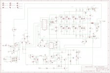
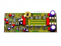
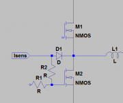
i am nearly completing my project, i chose ucd because of its stability . but i prefer the sound of non ucd. my development is below . i have used multipe outputs to handle heavy loads like bridge mode with 2 ohms. also added a zeener d8 at ir2110 between vb and vs to help with latching issues.
the protection is borrowed from manoj's wonderful amp aud600. (personally i liked it because it monitors both + ve and -ve rails and having build aud600 the protection works great)
i am open to ideas which will improve performance including noise reduction and stability.
>>>i am planing to use a maxx of +/-85 vlts with irfb4227/irfb4229 load 2ohms or
>>> a maxx of +/-65vlts with irf640n load 2ohms
enjoy...
First I was wondering why not, but checking the data sheets of IR2110/3 or IR2011 shows that they have no internal zener clamp for VB.
Agreed in this case you would need the said resistor and a 15V zener between VB & VS.
Other wise you can get overvoltage to VB and cause malfunction+defect.
My apologies to Steve that I did not check in detail first.
For IRS20957 and similar this diode is integrated and the external resistor is working great without additional zener diode. I am using this method in multiple designs and it is an absolutely troublefree easy going.
Also I learned from another chip brand that dv/dt of VB-VS can be headache, so I am generally using a dv/dt limitation for VB-VS. Details of my standard circuit to provide VB can be seen in my 2kW thread.
With respect to the link of jlester87 it is clear that this can also be headache with IR.
http://www.irf.com/technical-info/designtp/dt99-7.pdf
More general hint to tackle start up issues:
Usually proper starting depends on having the right preconditions at the comparator input ==> means ensuring that the amp wants to turn ON the low side switch first.
Or if this is not appreciated for audisoteric reasons, then you have to ensure that also the floating high side gate drive supply is charged without having turned ON the low side before.
Did your IRS900 fail at startup? If yes it's possible that you have a startup problem described here. Check the time constant of your bootstrap supply...
Since IRS900 doesn't have overcurrent protect, high side latching at startup will cause both mosfets to blow.
Now you passed the basics, here it comes the details. However I tried to explain these details at a dummy level, so more can understand it.
I reccomended you to lower swithcing frequency, and also your filter cutoff frequency, so itt will cut some material at >10kHz. However it is neccessary to lower swithcing freq, because you cannot buy modern (like IRFB4227) FETs.
I reccomend biamping, driving the tweeters with class-B amps, which need lower power.
Also Class D amps have a complex THD versus power curve:
- At lower power noise dominates, this is true for alla mps
- At medium power you have the THD fllor, which is a complex function of your layout, dead-time settings, swithcing noise reduction etc...
- At voltage outputs of about 70-90% of the supply rails a new phenomenon starts kicking it. It is called modulation error. Your amplifier has a input to output propagation delay (sum of the propagation delays of all parts). A Class-D amp has problem producing shortes pulses than the propagation delay.
It can be easily understood: your amplifier feedback loop watches the output and feeds back an error signal to input and so varies inputs so that output should have no error. However its control has a delay, so if it has to use control singals shorter then its operation delay, its starts producing errors.
So if you have a rails of +/-70V then you signal starts to have some distortion over 50-60V, a bit before the supply rails. This is normal. To reduce this it is neccesary to decrease the propagation delay of the amplifier (if it can answer faster,it will produce less error).
I managed this by using a full-bridge with no level shifting (so no extra delay of the leverl shifrter), a much faster comparator, and much faster gate driver IC.
This is the first elvel, to make the amplifier faster. The second level is to use an error amplifier. In the IRS2902 there is a built in error amplifier before the comparator.
Let's get back to the operation of the feedback network: the feedback network feeds back the output to produce an erros signal for the control to fix the output. An error amplifier works in two way:
- At noraml oruput it does nothing, however when modulation error start, it amplifies the error, so the control has an easier job correcting it.
- An input comparator delay is proportional to the input overdrive (whcih corresponds to the error signal). So the error amplifier not only helps by amplifiing error, it also decreases propagation delay. It does a dual job.
Due to the built in error amplifier the IRS2902 can operate at small distrotion up to high modulation indexes. This is some explanation for higher clarity.
Howver UcD is a post-feedback scheme, so the feedback also correct error of the output filter network, like:
- hich frequency boost/cut at some load impedances of the the LC filter (UcD has a much flatter freq response)
- nonlinearities of the output inductor (very bad cores not only dissipiate, but can increase distortion too)
- Output inpedance of the inductor (can be significant at high frequencies)
etc...
Hope you liked this post.
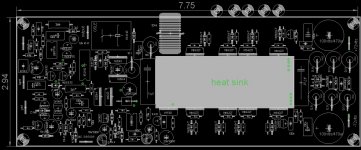
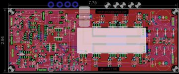
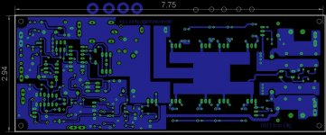
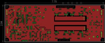
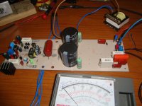
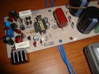
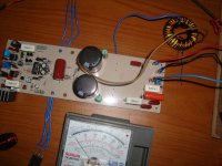
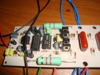
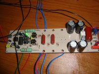
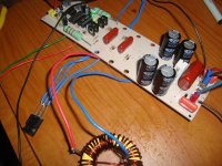
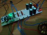
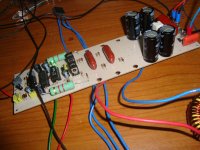
i am nearly completing my project, i chose ucd because of its stability . but i prefer the sound of non ucd. my development is below . i have used multipe outputs to handle heavy loads like bridge mode with 2 ohms.
also added a zeener d8 at ir2110 between vb and vs to help with latching issues.the protection is borrowed from manoj's wonderful amp aud600. (personally i liked it because it monitors both + ve and -ve rails and having build aud600 the protection works great)
i am open to ideas which will improve performance including noise reduction and stability.
>>>i am planing to use a maxx of +/-85 vlts with irfb4227/irfb4229 load 2ohms or
>>> a maxx of +/-65vlts with irf640n load 2ohms
enjoy...
Attachments
-
gtG ucd 1100 rev 2.0 schema .pdf48.7 KB · Views: 629
-
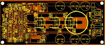
 gtG ucd 1100 rev 2.0 board components developement.jpg148 KB · Views: 2,146
 -
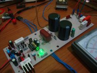
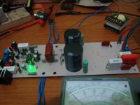
 gtG ucd 1100 rev 2.0 board full developement.jpg214.4 KB · Views: 2,049
 -
 gtG ucd 1100 rev 2.0 board pcb bottom developement.jpg142.1 KB · Views: 1,954
 -
 gtG ucd 1100 rev 2.0 board pcb top developement.jpg138.8 KB · Views: 1,863
 -
 gtG ucd 1100 rev 2.0 board schematic developement.jpg405 KB · Views: 1,994
 -
 gtG ucd 1100 rev 2.0.jpg88.3 KB · Views: 1,137
Ravpreet, Triell use a UCD clon from Eduardo Tagle an Argentinian ingeneer use transistor(5401 or mpsw92)
in level shifter, (irs use ic),and the comparator use lm311 (irs use tl081) and diference in the oscilattion mode ,the output its similar ,ir2110 ,Triell use bd136 to help the mos and irs 1500 don use (if use more vmos help use a pairs bd139-140) for more power (see the anterior Stewin post)
Change the carrier in Triell a capacitor in feedback, and irs a resistor,the mistake in Naridgi test tis a long wire betwen vmos and pcb
Stewin:
Why using IRFB4227 MOSFETs with 20mOhm Rdson, when you put 0,1 Ohm resistors in series with them.
The MOSFET driving network is also very ineffective. 47 OHm turn-on resitors can be good for <100kHz. Also BD243 and BD244 is way too slow. Layout is very poor. Some advices:
- Use a pair of very fast SOT-23 SMD transistor to boost gate drive (for example MMBT2222A and MMBT2907A is good) rigth next to the MOSFETS. Use a ceramic cap to filter the supply of these SMD BJTs. This will decrease the gate drive length extremely. So less inductance, faster driving, less noise.
- Forget the shunt protecting, it will have more loss than all other parts of the amplifier! Use the FETs for shunt, previousle I posted a simple schematic that does this, here it is again:

As you can see MMBT2907A boosts the turn off, and MMBT3904 the turn off, the first one is smaller.
U1 and U2 are the main FETs. When U2 turns on, the gate signal turns on the Q4 auxiliary FET (the 100 ohm resistor is for this FET should turn on a bit later). The R2 and C1 filters the swithced half bridge signal for spikes. IF the votlage drop at U2 main FET is at least 0,6V (about 20-30A per IRFB4227) it turns on Q3. The output signal from its collector then can be fed to an 555 timer to turn on protection.
The aux FET should have a very small Qgate and Coss, Rdson does not matter.
- Snubber desing is also very bad. RC snubber should be as close to the FETs as possible (1 RC snubebr per FET), because in reality it is an RLC snubber, if L is too big, it will help nothing, it will only make thing worse.
Still lot to learn
Why using IRFB4227 MOSFETs with 20mOhm Rdson, when you put 0,1 Ohm resistors in series with them.
The MOSFET driving network is also very ineffective. 47 OHm turn-on resitors can be good for <100kHz. Also BD243 and BD244 is way too slow. Layout is very poor. Some advices:
- Use a pair of very fast SOT-23 SMD transistor to boost gate drive (for example MMBT2222A and MMBT2907A is good) rigth next to the MOSFETS. Use a ceramic cap to filter the supply of these SMD BJTs. This will decrease the gate drive length extremely. So less inductance, faster driving, less noise.
- Forget the shunt protecting, it will have more loss than all other parts of the amplifier! Use the FETs for shunt, previousle I posted a simple schematic that does this, here it is again:
As you can see MMBT2907A boosts the turn off, and MMBT3904 the turn off, the first one is smaller.
U1 and U2 are the main FETs. When U2 turns on, the gate signal turns on the Q4 auxiliary FET (the 100 ohm resistor is for this FET should turn on a bit later). The R2 and C1 filters the swithced half bridge signal for spikes. IF the votlage drop at U2 main FET is at least 0,6V (about 20-30A per IRFB4227) it turns on Q3. The output signal from its collector then can be fed to an 555 timer to turn on protection.
The aux FET should have a very small Qgate and Coss, Rdson does not matter.
- Snubber desing is also very bad. RC snubber should be as close to the FETs as possible (1 RC snubebr per FET), because in reality it is an RLC snubber, if L is too big, it will help nothing, it will only make thing worse.
Still lot to learn
another class d amp test srimodify 3200.
Is this a Class-D amp? If this is really a Class-D amp it must be really bad.
Just look at the layout, it represents a typical layout of a Class-B amp.
For a Class-D amp easy heatsinking shoud not be a priority!
Priority is always small paths for sensitive signals. Double layer layout with a big ground plane is a must
Every cm of path is about 4nH parasitic inductance.
do u have any high power class d amp layouts u mentioned here.
thanks lorylaci . i want to use ucd to drive 1ohm stable at +/-85volts .i also included the protection schema to avoid latching  which has proved to be a pain in my experiences.
please can you draw and post an example of a schema which can drive 1ohm load in ucd mode at +/-85volts with protection . output fets to be irfb4227or irfb4229 because of their current ability.
also i do have mmbt 5401 and mmbt 5551 can they be used for boosting the gate drive?
which has proved to be a pain in my experiences. please can you draw and post an example of a schema which can drive 1ohm load in ucd mode at +/-85volts with protection . output fets to be irfb4227or irfb4229 because of their current ability.
also i do have mmbt 5401 and mmbt 5551 can they be used for boosting the gate drive?
Last edited:
hi exflacoRavpreet, Triell use a UCD clon from Eduardo Tagle an Argentinian ingeneer use transistor(5401 or mpsw92)
in level shifter, (irs use ic),and the comparator use lm311 (irs use tl081) and diference in the oscilattion mode ,the output its similar ,ir2110 ,Triell use bd136 to help the mos and irs 1500 don use (if use more vmos help use a pairs bd139-140) for more power (see the anterior Stewin post)
Change the carrier in Triell a capacitor in feedback, and irs a resistor,the mistake in Naridgi test tis a long wire betwen vmos and pcb
thanx for valuable detail
(see the anterior Stewin post) plz sir mention post no.
thanks lorylaci . i want to use ucd to drive 1ohm stable at +/-85volts .i also included the protection schema to avoid latching
please can you draw and post an example of a schema which can drive 1ohm load in ucd mode at +/-85volts with protection . output fets to be irfb4227or irfb4229 because of their current ability.
also i do have mmbt 5401 and mmbt 5551 can they be used for boosting the gate drive?
If you want power, the scheme is trivial. Keep in mind that not only half bridge, but FULL-BRIDGE Class-D amps also exists, and in lot of respect, they are much better. (There better FETs at =<150V range).
Do not be upset, but stewin you are weak now for an amp of +/-85V supply and 1 ohm load... You need to learn much more for that! The schematic and layout you posted was a way too bad for that.
MMBT5401 and MMBT5551 are not good. Keep in mind that this transistors will switch the gates at >1A, so they must have a reasonable current gain (>10) at a very high speed.
The BDs can provide lot of current, but the time they need to bring current up to 3A from 0, is much more, than the time the gates need to be discrahged (and charged, but dischare shoudl be much faster).
As I said your outdated protection scheme (shunt) will dissipate way more than anything else. The efficiency will suffer greatly.
I will continue later...
I will continue later...
Some of you wanted me to post a schematic and a layout. I post some picture examples and measurements.
Here is my last amplifier:


You can clearly see the use of double-side layout with big ground-plane, and the heavy use of SMT components. This enable efficienty use. With only 30-40ns set dead-time, the no-load current consumption is about 20mA from the high rail (72V, so about 2W idle loss). This means no cross-conduction, and the small dead-time also gives less THD and noise.
Here are to outputs of the half-bridges:

As you can see the good switching and the efficient snubber (SMT components mounted right next to the FETs) eliminates all ringing, and the shot-thorugh is also really small. The next measuremtn is the output after the LC filter:

As you can see the swithcing transient is greatly reduced at the output. This can be only achieved by controlled switching, and a fitler with low parasitics (the inductor is a gapped ferrite wound in one layer of special-formed wire).
This transients leak back to the input giving white noise. If they are elminiated at the ouput, you will have an easy job at the input. This amp is really noise-less.
This a full bridge amp operatiing from 60-75V. I use FDP3652 FETs (Rdson=14mOhm, Gate crhage 40-50nC, low Coss), which I get about 1$/piecs. With this FETs I can drive 8 Ohm with that small aluminum profile. With expanded hetasinkink (a small heatsink with fan mounted at the top) it can drive 4 Ohm and 2Ohm.
Good design thanks post
my next project irs4k5 ,
designing not finished yet.
- Home
- Amplifiers
- Class D
- UCD 25 watts to 1200 watts using 2 mosfets