Sorry Frank, I wasn't crediting Mike with the link, but didn't see him putting it up before I put it up myself.
There's no correspondence between the four topologies and the CFB/VFB terminology. The four concepts concern itself with what you sample at the output (current or voltage) and how you add the feedback signal to the input signal (in series or shunt/parallel). The reason is that this immediately shows the effect on the amp: decreased or increased output Z, and increased or decreased input Z.
The CFB/VFB terminology came en vogue after Elantec designed the first opamps with a low-impedance (emitter) feedback node which had some favourable effects on the bandwidth and called it current feedback. Must have been late 70's? But it doesn't say anything about the effect of the feedback on the amp, because you can still use this 'CFA' with either current or voltage output sampling to make an amp with zero or infinite Zout.
So we're stuck with two different ways of looking at feedback, which have no correspondence.
jan
O.k. I can understand that. This makes talking about CFB/VFB a bit of a problem, there are 4 (IMO 5
") but I may be wrong) topologies and 2 acronyms, something has to change?
but I may be wrong) topologies and 2 acronyms, something has to change?And still, if CFB/VFB are valid terms (in some way) I (for one) would be interested in how to apply the terms to the 4 models. IMO 4a is VFB, 9a is CFB and I do not have definite designations for the other models.
If we would give definite designations to the models, we may even draw different models (I am willing to do that) it would be easier to discus about them (my thought). Lets create some common reference.
Frans.
.jpg")

O.k. I can understand that. This makes talking about CFB/VFB a bit of a problem, there are 4 (IMO 5
And still, if CFB/VFB are valid terms (in some way) I (for one) would be interested in how to apply the terms to the 4 models. IMO 4a is VFB, 9a is CFB and I do not have definite designations for the other models.
If we would give definite designations to the models, we may even draw different models (I am willing to do that) it would be easier to discus about them (my thought). Lets create some common reference.
Frans.
I don't think that is possible, the methods of naming have different starting points, as I tried to explain. You'd decide what kind of amp you want, like you want a low Zout and a high Zin, that would be shunt-shunt feedback, and then you go about the actual implementation and you can chose 'CFB' or 'VFB' depending on specific targets. So the two sets are completely independent.
jan
....Certainly the forward voltage gain of the first device looking from the non-inverting input (vs) to ground is not gmRc ????
I didn't say it wasn't!
Voltage gain of a common emitter amplifier=gm*Rload=Rload/re; Where gm=1/re.
Now, in a so-called "CFA", re is in series with (and swamped by) the Thevenin impedance, Re, of the feedback voltage divider as seen from the input stage's emitter so that
Voltage gain of the first stage~Rload/Re.
Thus, When Re is increased by, for instance, increasing the value of the grounded resistor of the feedback network, the "CFAs" forward path gain is reduced and the apparent bandwidth is reduced; closed loop gain is also reduced.
I hope this is clear.
Last edited:
The current that drives the gain node i.e. the Ccomp flows in the feedback network. Can you deny this (that's where the high slewrate comes from to)?
High slew occurs in "CFA" arrangements in which two complementary common emitter transistors are connected in parallel (emitter to emitter).
The input stage then operates in class AB when required to meet the current demands of the shunt (grounded) compensation capacitor.
The current that drives the compensation capacitor does not flow in the feedback network: the two are isolated by the output buffer.
I didn't say it wasn't!
I hope this is clear.
I just pointed out that that reference does not have the feedback resistance in the forward gain (at least in the equations).
I frankly don't know what all the fuss is about, taking this simple circuit and setting up the H parameter representation of A and f makes everything so clear. The flow diagrams and simplifications are not necessary.
The current that drives the compensation capacitor does not flow in the feedback network: the two are isolated by the output buffer.
Yes it does as do all error currents. The current that slews the capacitor does but the signal displacement current doesn't. It comes out the emitters (-input) where does it go? The capacitor is usually to ground (simple folded cascode).
It comes out the emitters (-input) where does it go?
True, at least partly:
One half of the complementary input stage sources current to drive the compensation capacitor while the other half sinks it, except where the input stage is forced to operate in class AB, in which case the feedback network must sink or source current.
Last edited:
I don't think that is possible, the methods of naming have different starting points, as I tried to explain. You'd decide what kind of amp you want, like you want a low Zout and a high Zin, that would be shunt-shunt feedback, and then you go about the actual implementation and you can chose 'CFB' or 'VFB' depending on specific targets. So the two sets are completely independent.
jan
Then I am (was always) wrong, looking at 4a you see an amplifier that changes the voltage at opamp-in(+) and opamp-in(-) in unison, this for me was the sign of an voltage-feed-back configuration. Figure 9a shows an situation where (more or less (minus the error signal)) the voltage at opamp-in(+) and opamp-in(-) is always at 0(zero) volts, that has always been (for me) the signature of an current-feed-back amplifier.
I frankly don't know what all the fuss is about, taking this simple circuit and setting up the H parameter representation of A and f makes everything so clear. The flow diagrams and simplifications are not necessary.
Different way to skin a cat. I sometimes prefer to use signal flow graphs (Mason's rule) to analyse feedback systems.
Then I am (was always) wrong, looking at 4a you see an amplifier that changes the voltage at opamp-in(+) and opamp-in(-) in unison, this for me was the sign of an voltage-feed-back configuration. Figure 9a shows an situation where (more or less (minus the error signal)) the voltage at opamp-in(+) and opamp-in(-) is always at 0(zero) volts, that has always been (for me) the signature of an current-feed-back amplifier.
See this:
http://www.diyaudio.com/forums/soli...current-feedback-amplifier-8.html#post3414948
True, at least partly:
One half of the complementary input stage sources current to drive the compensation capacitor while the other half sinks it, except where the input stage is forced to operate in class AB, in which case the feedback network must sink or source current.
Scott,
On reflection, the above statement is not correct; my mistake:
In fact, whether the input stage operates in class AB or class A is irrelevant: the feedback network must always source or sink current from the input stage's emitter(s).
Scott,
On reflection, the above statement is not correct; my mistake:
In fact, whether the input stage operates in class AB or class A is irrelevant: the feedback network must always source or sink current from the input stage's emitter(s).
No problem. Unfortunately my text won't scan and I'm not about to draw the whole thing. Anyway, if you decompose the circuit with H parameters the feedback network is in series with the input (Rg||Rf) and the hrf of the feedback network is Rg/(Rg+Rf). So the Vout*hrf at the input looks like a constant current Vout/Rf. I think the nomenclature is innocently derived from this.
Anyway, if you decompose the circuit with H parameters the feedback network is in series with the input (Rg||Rf) and the hrf of the feedback network is Rg/(Rg+Rf). So the Vout*hrf at the input looks like a constant current Vout/Rf.
...while Rg||Rf (the feedback network loading at the input inverting node) modifies the open loop gain (decreases with decreasing Rf), therefore providing the known sliding open loop gain crossover frequency. This dependency is also responsible for the "Rf provides frequency compensation" statement, encountered in CFA descriptions.
No problem. Unfortunately my text won't scan and I'm not about to draw the whole thing. Anyway, if you decompose the circuit with H parameters the feedback network is in series with the input (Rg||Rf) and the hrf of the feedback network is Rg/(Rg+Rf). So the Vout*hrf at the input looks like a constant current Vout/Rf. I think the nomenclature is innocently derived from this.
Can you post the schematic please? What is Rg, Rf and hrf?
...while Rg||Rf (the feedback network loading at the input inverting node) modifies the open loop gain (decreases with decreasing Rf), therefore providing the known sliding open loop gain crossover frequency. This dependency is also responsible for the "Rf provides frequency compensation" statement, encountered in CFA descriptions.
My mistake - should be increases with decreasing Rf
Can you post the schematic please? What is Rg, Rf and hrf?
Here
Fig. 39. Rg is 1k, Rf is 3.3k. Probably the simplest "CFA", also illustrating that the debate is 100% semantic. Nobody is, in fact, technically wrong.
Or on this forum, here. Rg is 47ohm, Rf is 1k.
hrf is the reverse transfer function of the feedback network, defined using the hij parameters (as canonical for a series - parallel feedback circuit)
Last edited:
Or on this forum, here. Rg is 47ohm, Rf is 1k
It's late here... actually 23.5ohm and 500ohm if you fold the AC equivalent schematic.
Caution: Participating in this thread could be hazardous to your forum membership!
Reading through it, I couldn't help noticing all the enthusiastic contributions by the following ex-members:
Reading through it, I couldn't help noticing all the enthusiastic contributions by the following ex-members:
- mikeks (Account Disabled)
- millwood (Account Disabled)
- Jocko Homo (Banned)
- Elso Kwak (Banned)
- jh6you (Account Disabled)
- andy_c (Banned)
- MalichiConstant (Account Disabled)
- microchip (Account Disabled)
- mastertech (Banned)
That too.This is probably the least necessary topic to revive.
Last edited:
Scott,
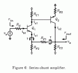
See fig 6 on pg 8 here:
http://users.ece.gatech.edu/mleach/ece3050/notes/feedback/fdbkamps.pdf
Also, read the text associated with this figure (section entitled "Transistor Example"); you should quickly realise that CFA is a complete misnomer, as it confirms everything I've said on the subject..Note that the table 1 on pg 2 corresponds with my definitions here:
http://www.diyaudio.com/forums/soli...current-feedback-amplifier-8.html#post3414948
Sorry MK, but fig. 6 on page 8 does not confirm you at all. Look at the input bjt Q1. It is an emitter follower. But the output bjt Q2 is a common emitter. This Q2 is different from the output stage of a CFA. The CFA output is an emitter follower, not CE. An EF has a low output impedance, a CE has a high Z. An EF output forces a constant voltage across the load and the feedback network. At the other end of the FB network, in a CFA, is the output of an EF, also a low Z output, buffering the input signal. With CFA, the fb current varies inversely w/ fb resistance. As Rf is lowered, If increases so that the cap is charged faster.
But looking at fig. 6, page 8, the output is a CE stage, i.e. the collector drives the fb resistor and load. This is high output Z constant current. Lowering Rf does not increase current as much as in the EF output stage. Rf and Rload divide the current, so that if Rf is lowered, the output voltage is lowered with Rf carrying a larger portion of the EF collector current.
The 2 outputs are quite different. Also, the input stage for a CFA is EF, not CE, not CB. The feedback current at the emitter node of the input EF can be said to stimulate the emitter of a CBstage. But the "gain" of this stage is NOT "Rload/Re". This stage drives a current mirror and the other branch drives the capacitor in the TIS. Hence even though you can argue that the input emitter node is driving the input buffer in CB or CE mode, the voltage at the collector is not the stage output, rather collector current is.
Here is my summary on this subject. For audio, I am not convinced that CFA is a better choice than VFA. I haven't tested them so I cannot say if one is better. Maybe I'm prejudiced, but for audio frequencies, I would favor the VFA. A VFA has lower output error due to input current amd voltage offsets. Also, the error due to bias/offset current can be reduced with proper R value in the noninverting input.
The emitter coupled pair in a VFA input is really good. The ecp would not be the only game in town for 6 decades if it were not the best. It rejects differential input errors/noise, has only 2 devices requiring matching, provides 1 terminal for input, another for feedback, very good topology. CFA is great at video speeds, and where low frequency and dc performance are not as critical. So if I had to develop an audio amp, I would evaluate both, but VFA is what I now favor.
Regarding terminology, CFA is the only correct nomenclature, and calling it VFA is merely an attempt to force every electrical entity into a voltage mode modus operandi. The same people calling the CFA a misnomer also insist that all or most devices classified as "current-driven/controlled" are also misnomers. They cannot accept current as a control or error signal.
All for now, I will answer questions or elaborate if needed. I ask interested parties who differ with me to scroll back to my posts from 2004-06, and view my schematic which clearly illustrates that "CFA/CFB" is the only proper name.
The output voltage is usually the sampled quantity, but the op amp is classified as to how it develops the servo wrror signal. A VFA usually senses the output voltage and feeds it back. But "VFA" refers to the error signal controlling the loop action. A VFA can be used to sense output current through feedback. A motor driver, LED driver does this. A low values resistor is placed in series with the higher resistance load. The resistor voltage is fed back. But the output is current. The VFA has a high Z input, it cannot input the load current directly, so the sense resistor translates the output current into a voltage. The VFA must receive its input as a voltage.
So the overall network is current fb, but the op amp is VFB, so that a resistor translated I to V, and all is well. Just because the sampled output quantity is current, the maker of the op amp must specify it as VFB. The sampled output could be either, I or V, or temperature, frequency, strain, etc.
Likewise with CFA, the sampled output quantity is generally voltage, but it ccould be other. The CFB topology translates output V into an I which is the error signal driving the servo loop. I explained how in 2004-06. Best regards.
Claude
Q1 and Q2 are both common emitter stages.Sorry MK, but fig. 6 on page 8 does not confirm you at all. Look at the input bjt Q1. It is an emitter follower. But the output bjt Q2 is a common emitter.
Attachments
- Status
- This old topic is closed. If you want to reopen this topic, contact a moderator using the "Report Post" button.
- Home
- Amplifiers
- Solid State
- Current feedback - Voltage feedback, how do I see the difference?