How did you get video of my Christmas?
Measurement of bias current and bias stability. .
As drawn, Rs has no action on Vgs, so, how does it stabilizes?
Today I saw an article describing the JBL SD-400 'Energizer', with a transformer coupled driver stage. It uses a diode (1N2326 - COMPENSATING DIODE, as a Zener of 1V, as far as I understand) to get a bias across the two output windings to the Base of two parallel output NPN transistors 2N2147 per half.
It does have a bootstrap cap to the bias resistor feeder network (225 ohm/250 uF/225 ohm drawing a bias current of about 70 mA) but there is no signal there.
This is an alternative technology for the bias.
- It looks very much like the conceptual F6 schema of NP with his circle with a V in it denoting the bias;
- though much more sophisticated and compensated for real life signals, it resembles Radford's schema (post 146 on p 14)
It does have a bootstrap cap to the bias resistor feeder network (225 ohm/250 uF/225 ohm drawing a bias current of about 70 mA) but there is no signal there.
This is an alternative technology for the bias.
Is it a current article introducing a new amp?Today I saw an article describing the JBL SD-400 'Energizer', with a transformer coupled driver stage. It uses a diode (1N2326 - COMPENSATING DIODE, as a Zener of 1V, as far as I understand) to get a bias across the two output windings to the Base of two parallel output NPN transistors 2N2147 per half.
It does have a bootstrap cap to the bias resistor feeder network (225 ohm/250 uF/225 ohm drawing a bias current of about 70 mA) but there is no signal there.
- It looks very much like the conceptual F6 schema of NP with his circle with a V in it denoting the bias;
- though much more sophisticated and compensated for real life signals, it resembles Radford's schema (post 146 on p 14)
This is an alternative technology for the bias.
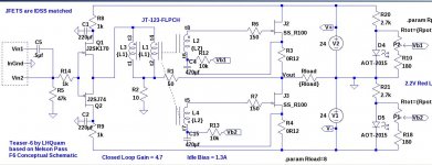
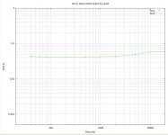
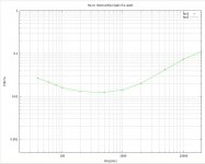
I have modified by stereo Teaser-6 to eliminate source degeneration, thus increasing open-loop gain and damping factor. Show are the new schematic, and THD vs. Frequency at 1 watt into 8 ohms for the left and right channels. You should not the vast difference between the two channels. The right channel probably has an inferior SemiSouth R100 JFET. The closed-loop gain is about 4.7.
I measured the output impedance Zo=0.4724 and damping factor DF=8/Zo =16.9. Zo is about 1.5X the value predicted by Spice, perhaps because of differences between the JFET model parameters (Gm) and the actual devices.
After listening for a while, the tonal issues that were probably related to damping factor are mostly gone, but the harmonic distortion is noticeable and objectionable.
Attachments
Last edited:
As drawn, Rs has no action on Vgs, so, how does it stabilizes?
Rs is outside modulation circ, but inside bias circ
i am in the mist.
Some help?
Rs is important from two reasons - bias stability , and dynamic influence .
you can delete entire modulation mechanismus ( xformer) and Rs is still in place where needs to be , regarding bias and it's stability
dynamic influence - even if not accounted in xconductance of part itself , it ads to output impedance of amp , contributing to THD form
i am in the mist.
Some help?
The following is the understanding I noted among the participants.
- The resistor R source [Rs] is not required for thermal stability as JFETs have a negative temperature coefficient.
- The abscence of source resistor Rs maximizes gain of output stage; very much needed to be sacrificed so as to lower Zo.
- A source resistor Rs increases Zo. Wrong way.
- Need to/must sense the bias/idle current of JFETs to set operating point.
Attachments
Actually the SemiSouth literature refers to a positive temperature coefficient, meaning effective resistance of the FET increases with temperature, and the current decreases.
The sense resistor can be on the source leg of the FET if the connection to the capacitor in the bias circuit is above it as shown in post #1647 http://www.diyaudio.com/forums/pass-labs/216616-f6-amplifier-165.html#post3159810. And yes, only one sensor resistor is essential. But, bias stability is improved by having 2 sense resistors as shown in post #1626 http://www.diyaudio.com/forums/pass-labs/216616-f6-amplifier-163.html#post3159277, where the bottoms of the bias generator diodes are referenced to voltages below the sense resistors.
The sense resistor can be on the source leg of the FET if the connection to the capacitor in the bias circuit is above it as shown in post #1647 http://www.diyaudio.com/forums/pass-labs/216616-f6-amplifier-165.html#post3159810. And yes, only one sensor resistor is essential. But, bias stability is improved by having 2 sense resistors as shown in post #1626 http://www.diyaudio.com/forums/pass-labs/216616-f6-amplifier-163.html#post3159277, where the bottoms of the bias generator diodes are referenced to voltages below the sense resistors.
The following is the understanding I noted among the participants.
The attached schematic looks at ZM's earlier explanations in a different way. A resistor is put the drain circuit of each JFET; strictly to sense bias current. This takes care of the above 4 points. Actually, if one does not care about symmetry, the Rsense in the circuit of the upper or lower JFET is the only one needed. The current flowing through both JFETs is the same.
- The resistor R source [Rs] is not required for thermal stability as JFETs have a negative temperature coefficient.
- The abscence of source resistor Rs maximizes gain of output stage; very much needed to be sacrificed so as to lower Zo.
- A source resistor Rs increases Zo. Wrong way.
- Need to/must sense the bias/idle current of JFETs to set operating point.
Last edited:
Thank you lhquam for clarifying the meaning and desirable value of the +ve temp coefficient of JFEts. There is also another simple method to adjust bias current in the output stage which totally excludes a sense resistor [anywhere] in the output circuit. Sense the AC current with a clip on multimeter which enters the primary or exits the secondary of the power transformer feeding the amp's power supply. One can also do both [i.e. use R sense in the output stage, and simultaneously AC sense] so as to generate a calibration plot and use AC sense as the default method.Actually the SemiSouth literature refers to a positive temperature coefficient, meaning effective resistance of the FET increases with temperature, and the current decreases.
The sense resistor can be on the source leg of the FET if the connection to the capacitor in the bias circuit is above it as shown in post #1647 http://www.diyaudio.com/forums/pass-labs/216616-f6-amplifier-165.html#post3159810. And yes, only one sensor resistor is essential.
How would that work with a pair of stereo channels sharing power supplies? Another scheme is to have a "switch" consisting of a screw thru the PCB whose head is soldered a supply trace. On the other side a nut makes contact with the trace supplying the FET power. For bias adjustment the nut is loosened and an ammeter is connected to the two traces. I did something similar in the this thread: http://www.diyaudio.com/forums/pass-labs/213152-balanced-f5-small-footprint.html#post3033456.
Thank you lhquam for clarifying the meaning and desirable value of the +ve temp coefficient of JFEts. There is also another simple method to adjust bias current in the output stage which totally excludes a sense resistor [anywhere] in the output circuit. Sense the AC current with a clip on multimeter which enters the primary or exits the secondary of the power transformer feeding the amp's power supply. One can also do both [i.e. use R sense in the output stage, and simultaneously AC sense] so as to generate a calibration plot and use AC sense as the default method.
You have a facile solution to exclude sense/source resistors from the output stage and simultaneously adjust the idle current.How would that work with a pair of stereo channels sharing power supplies? Another scheme is to have a "switch" consisting of a screw thru the PCB whose head is soldered a supply trace. On the other side a nut makes contact with the trace supplying the FET power. For bias adjustment the nut is loosened and an ammeter is connected to the two traces. I did something similar in the this thread: http://www.diyaudio.com/forums/pass-labs/213152-balanced-f5-small-footprint.html#post3033456.
I built the Silencer 
Music in one end, silence out the other. Must have been too excited from kids Futbol game and screwed up somewhere. All biases well, and AC signal can be read across primaries, but secondaries are a hush hush affair. Oh well, tomorrow. Sleepy time.
Note to self. SLow DOwn!
Music in one end, silence out the other. Must have been too excited from kids Futbol game and screwed up somewhere. All biases well, and AC signal can be read across primaries, but secondaries are a hush hush affair. Oh well, tomorrow. Sleepy time.
Note to self. SLow DOwn!
You have a great achievement. Think of the advantages.
Hum and noise: ZERO
THD: ZERO
")
Hum and noise: ZERO
THD: ZERO
I built the Silencer
Music in one end, silence out the other. Must have been too excited from kids Futbol game and screwed up somewhere. All biases well, and AC signal can be read across primaries, but secondaries are a hush hush affair. Oh well, tomorrow. Sleepy time.
Note to self. SLow DOwn!
Not sure I should refer to him as Papa, being 7 years his senior.
Papa has been awfully quiet lately. Did he forget to pay is ISP?
I am getting to like the sound of the Teaser-6. It sounds quite different from the F5 and F5-balanced.
The low end in more pronounced. I do not know it that is due to higher transconductance FETs or harmonic distortion. Is not due to a bump in low end frequency response.
The stereo imaging is very good.
The high end seems to be fine, but my old ears cannot be relied on for judging this.
There is some noticeable distortion in the mid frequencies, but I am getting more tolerant to it.
Time will tell. If I am still happily listening to it in a week, then I would say it is a keeper.
- Home
- Amplifiers
- Pass Labs
- F6 Amplifier