I am about to embark on my first amp build! I have used a design based on a design from The Audiophile Sourcebook by G. Randy Slone. I have re-created the schematic in Eagle based on the components I was able to procure and did the board layout myself.
I am looking for feedback on my overall layout and the base design. As this is my first amplifier build, I'm hoping all of you seasoned veterans can give me some tips to help me along the way and correct any stupid mistakes I may have made") Thanks in advance for any advice you can provide.
Thanks in advance for any advice you can provide.
I am looking for feedback on my overall layout and the base design. As this is my first amplifier build, I'm hoping all of you seasoned veterans can give me some tips to help me along the way and correct any stupid mistakes I may have made
Thanks in advance for any advice you can provide.Attachments


Randy's non-polarised caps
Perhaps due to his parts company's stocking policy, the late Randy Slone always specified and illustrated non-polarised electrolytic caps as two back-to-back electros of twice the required value.
I believe that's little different to how they are electrically arranged in commercial parts anyway.
Perhaps due to his parts company's stocking policy, the late Randy Slone always specified and illustrated non-polarised electrolytic caps as two back-to-back electros of twice the required value.
I believe that's little different to how they are electrically arranged in commercial parts anyway.
Why two electrolytic caps in the input... C12/C10?
Yeah, I went back and forth about the input caps as well.
My understanding was that they act as input coupling capacitors that block any DC signals at the input. However, I also know that having the signals pass through an electrolytic like this seems to be generally frowned upon. Since it is my first build, I decided that more protection was better than less. What do you think?
The circuit does not appear to be correct.
How is the input connected to the output?
It looks like an attempt to do a symmetrical input with current mirrors, except they aren't connected to the output.
This is a problematic circuit even when there is a connection.
A search will turn up multiple threads on the topic.
The problems are soluble but need care.
You should read Robert Cordell's book for this.
Best wishes
David
Last edited:
Why two electrolytic caps in the input... C12/C10?
It's a way of creating a bi-polar electrolytic cap using two cheaper polarized ones. Personally I don't like electros of any type in the signal path. (feedback input is also a signal path
)I think there are a couple connections missing in the schematic.
 Check the bases of T2 & 21.
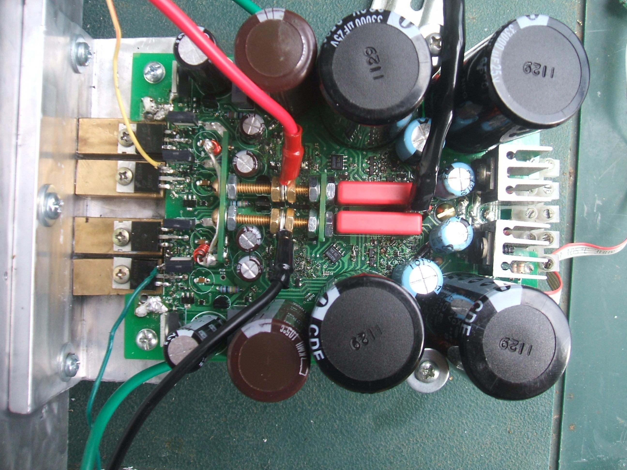
 There are circuit paths on the pcb that have to carry large currents, not constant but large transient currents. These paths must be wide enough to carry the current with minimal effect to the circuit and they must be placed so as the magnetic field that is generated by this large transient current doesn't affect the higher impedance traces that are close by. Decoupling should be close to the output stage. You want to try to 'star' the grounding paths. This is important to keep the voltage drop of the ground trace of one circuit from not affecting another. Here is an example of a stereo amplifier, at least with regard to the high current paths where the power supply is on the same pcb. PS is C-R-C-C-c-Cfilm. The 34VAC CT 17.6V-0V-17V power transformer connects to the three holes on the left connecting to the TO-220 rectifier diodes. photo1 photo2 The high current paths flow around the outside through wide traces to the output transistors by way of a mosfet switch and the heatsink tab and then output through the brass screws to each speaker wire that returns to a brass screw at the center ground between the final large caps. The other circuitry gnd returns have their own path back to the 'star' point.
Last edited:
It's a way of creating a bi-polar electrolytic cap using two cheaper polarized ones. Personally I don't like electros of any type in the signal path. (feedback input is also a signal path
I think there are a couple connections missing in the schematic.
There are circuit paths on the pcb that have to carry large currents, not constant but large transient currents. These paths must be wide enough to carry the current with minimal effect to the circuit and they must be placed so as the magnetic field that is generated by this large transient current doesn't affect the higher impedance traces that are close by. Decoupling should be close to the output stage. You want to try to 'star' the grounding paths. This is important to keep the voltage drop of the ground trace of one circuit from not affecting another. Here is an example of a stereo amplifier, at least with regard to the high current paths where the power supply is on the same pcb. PS is C-R-C-C-c-Cfilm. The 34VAC CT 17.6V-0V-17V power transformer connects to the three holes on the left before the TO-220 rectifier diodes. photo The high current paths flow around the outside through wide traces to the output transistors by way of a mosfet switch and the heatsink tab and then output through the brass screws to each speaker wire that returns to a brass screw at the center ground between the final large caps. The other circuitry gnd returns have their own path back to the 'star' point.
Wow, you are totally correct
That is a really stupid mistake. I missed a connection from the output of T16 to the base of T21 and the same on T7 and T2. I'll upload a some new pics.Updated Schematic and Board
I have updated my design to fix the mistake that was pointed out regarding the connection of the IPS to the VAS.
Really stupid mistake on my part. Sorry about that guys, still learning...
I have updated my design to fix the mistake that was pointed out regarding the connection of the IPS to the VAS.
Really stupid mistake on my part. Sorry about that guys, still learning...
Attachments


It's a way of creating a bi-polar electrolytic cap using two cheaper polarized ones. Personally I don't like electros of any type in the signal path. (feedback input is also a signal path
I think there are a couple connections missing in the schematic.
There are circuit paths on the pcb that have to carry large currents, not constant but large transient currents. These paths must be wide enough to carry the current with minimal effect to the circuit and they must be placed so as the magnetic field that is generated by this large transient current doesn't affect the higher impedance traces that are close by. Decoupling should be close to the output stage. You want to try to 'star' the grounding paths. This is important to keep the voltage drop of the ground trace of one circuit from not affecting another. Here is an example of a stereo amplifier, at least with regard to the high current paths where the power supply is on the same pcb. PS is C-R-C-C-c-Cfilm. The 34VAC CT 17.6V-0V-17V power transformer connects to the three holes on the left connecting to the TO-220 rectifier diodes. photo1 photo2 The high current paths flow around the outside through wide traces to the output transistors by way of a mosfet switch and the heatsink tab and then output through the brass screws to each speaker wire that returns to a brass screw at the center ground between the final large caps. The other circuitry gnd returns have their own path back to the 'star' point.
Hmm. If I understand this correctly, you are suggesting that I move the power supply inputs and the decoupling caps up closer to the output transistors and beef up my traces a bit in this area to accomodate the high current transients. If that is the case, that sounds like a good idea...
As far as star grounding, I plan on incorporating an external power supply that will incorporate a high-quality ground point for me to connect back to. This seems like it should be close to what you are suggesting.
Mr. Slone definitely designed the original amp as a single layer board So, single layer is definitely an option, but it would include closer traces and/or a larger board. Since I plan on having this board made for me, there isn't much of a cost savings associated with only doing a single layer. So, I'm thinking a 2-layer board is my best option.
So, single layer is definitely an option, but it would include closer traces and/or a larger board. Since I plan on having this board made for me, there isn't much of a cost savings associated with only doing a single layer. So, I'm thinking a 2-layer board is my best option.Mr. Slone definitely designed the original amp as a single layer board
Two sides is the way to go!
you will have more space to get thicker roads. also I would use just one input cap but a high quality cap.Hi,
Single layer enough
I designed a motor drive amplifier several years back +/- 35 volts peak currents over 12 amps which is not very different from an audio amplifier. It was done on a 4 layer bard with 2 ounce copper. Multi layer shouldn't be avoided because of unfamiliarity. It gives a lot of latitude with those magnetic fields and peak currents. Silk screen on both sides can make servicing easier. I've found, ironically, that making service easier often results in less service needed.
G²
Now you have drawn the collector of T7 connected to the base of the constant current source T8. That won't do it.
David
Sorry, I should have pulled that trace down a bit. The collector of T7 isn't connected to the base of T8, I just routed it through the connection
It actually doesn't connect until it hits the wire connecting to T2. Sorry for the confusion...I'm working on getting my decoupling caps closer to the output stage and increasing the size of the traces in the output. I'm going to move the connectors for the power supply up a bit too so that those traces have a shorter path to the output stage since that is where the current will be flowing. I'll upload a new board image when I get that finished.
Thanks a lot for the feedback so far! I don't know where I'd be without this forum...
Thanks a lot for the feedback so far! I don't know where I'd be without this forum...
Sorry, I should have pulled that trace down a bit. The collector of T7 isn't connected to the base of T8, I just routed it through the connection
Yes, I assumed that, That's why I said it was drawn that way. It was a rushed comment over lunch. But best to draw it correctly or else one day...!
Best wishes
David
Design Updates!
Finally got time to update the design based on some of the feedback. Basically, I have moved my decoupling caps up really close to the OPS and dramatically increased the size of the traces in the OPS to help accomodate the large transient current load that will be passed through.
While I was at it I also physically moved the OPS components away from the other stages and I went ahead and added a dedicated grounding point for the output devices that I can wire directly to my star ground.
The schematic has also been slightly modified to make it less confusing
Attachments


Better but still -
The output MOSFETs are drawn as bipolars.
The lower VAS connection is drawn over R32's GND.
As to the actual circuit.
The input LTP current is lower than recommended. Read D. Self for this.
The MOSFET stoppers could probably be lower. Cordell is the reference for MOSFETs.
The compensation capacitors could be swapped. Harry Dymond here.
Best wishes
David
but still -The output MOSFETs are drawn as bipolars.
The lower VAS connection is drawn over R32's GND.
As to the actual circuit.
The input LTP current is lower than recommended. Read D. Self for this.
The MOSFET stoppers could probably be lower. Cordell is the reference for MOSFETs.
The compensation capacitors could be swapped. Harry Dymond here.
Best wishes
David
Last edited:
Better
The output MOSFETs are drawn as bipolars.
The lower VAS connection is drawn over R32's GND.
As to the actual circuit.
The input LTP current is lower than recommended. Read D. Self for this.
The MOSFET stoppers could probably be lower. Cordell is the reference for MOSFETs.
The compensation capacitors could be swapped. Harry Dymond here.
Best wishes
David
None of this needed, looks like optimos, very good amp as is. Mods will change the sound and it sounds just fine.
- Status
- This old topic is closed. If you want to reopen this topic, contact a moderator using the "Report Post" button.
- Home
- Amplifiers
- Solid State
- First solid state amp design/build, advise