This patent [inventor Nelson Pass] taught STASIS {R} technology which was implemented in the power amps of Threshold Corp. I still have a Theshold S/150. At the time I bought it, it came with a complimentary copy of the granted patent. I 'll put Fig 2 in a pdf file in a following thread for the other DIYers to appreciate your point.Could this be an implementation of US Pat. 4,107,619 (Fig.2)?
Please find attached Fig. 2 of US 4,107,619.This patent [inventor Nelson Pass] taught STASIS {R} technology which was implemented in the power amps of Threshold Corp. I still have a Theshold S/150. At the time I bought it, it came with a complimentary copy of the granted patent. I 'll put Fig 2 in a pdf file in a following thread for the other DIYers to appreciate your point.
Attachments
I have a nice start but my setup seems to oscillate now at the drop of a hat - fried two more latfets... no clue why because the same setup with complementary outputs was very well behaved....
What value gate resistors are you using?
Last edited:
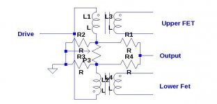
What inductances and turn ratios did you use in the transformer Spice model?An externally hosted image should be here but it was not working when we last tested it.
What value gate resistors are you using?
Hi there ... 220 ohms .... I'm just doing some changes now, but seems to me that the issue is quite simply that applying the signal from the outputs to the gate for the TOP fet is probably not a good idea - that fet is in a non inverting config so what I'm doing is applying positive feedback instead of negative feedback (for the top half ) almost ensuring that I get oscillations coming in at some point. I venture.
Bottom half is inverting , so issue doesn't crop up there.
Anyway, reconfiging the biasing with a bypass cap for the top half and taking bias ground from zero volts Instead of output to see if it works as I think it should.
Trying to learn at least through my own mistakes ......
to get additional inspirations by circuits with the use of a transformator for driving NPN/N-Channel BjT/MOSFET power devices,
check out the schematics from post #
54+79 (Vox Supreme), 55 (Rogers A75) and 83 (Altec 1590E)
about
http://www.diyaudio.com/forums/soli...-models-quasi-complementary-power-output.html
so as post #19 - 32 - 40 (Burns "Orbit Three") about
http://www.diyaudio.com/forums/parts/167680-vintage-transistors-2.html
have a look also to the attached files:
Attachments
Last edited:
wow .. fabulous appetizer while we await the main course - nicely done and phenomenal results !
Would love to hear how any breadboarded results go - I have a nice start but my setup seems to oscillate now at the drop of a hat - fried two more latfets
Please clarify the conditions of your test. Were the secondaries of the transformer driving the latfets in-phase according to the simplified F6 schematic? There are a total of four key experiments for a multiway comparison of amplifiers' performance.
- N [or P] channel output FETs driven in phase and out of phase
- Complementary N and P channel output FETs driven in phase and out of phase
supplement to post #269
http://www.google.com/patents/US5838196
http://www.google.com/patents/US5838196
Attachments
Last edited:
Complementary N and P channel output FETs driven in phase and out of phase
What am I saying! You and I cannot draw a schematic like the simplified F6 using complementary devices [per the earlier comment of kasey197; please clarify]; be it bjt or MOSFET. But I can do so with enhancement [top] and depletion [bottom] N-channel JFETs.
Please clarify the conditions of your test
. Were the secondaries of the transformer driving the latfets in-phase according to the simplified F6 schematic?
>>out of phase<<
- N [or P] channel output FETs driven in phase and out of phase
>>N channel, out of phase.<<- Complementary N and P channel output FETs driven in phase and out of phase
>>in phase, if out of phase all you see is the residual distortion coming from mismatches, ie no signal at the output<<
The signals to the output transistors are out of phase for/in each of the two amplifiers making the bridge. First; is there a specific precedent [schematic] in the open literature for in-phase drive, and secondly how is its performance compare with out of phase drive? That's the principal intrigue in/of F6!that's bridged output config
What am I saying! You and I cannot draw a schematic like the simplified F6 using complementary devices [per the earlier comment of kasey197; please clarify]; be it bjt or MOSFET. But I can do so with enhancement [top] and depletion [bottom] N-channel JFETs.
I'm not getting it
both types - depletion and enhancement - are "opening" more with rising voltage on gate (ref. source)
difference is just in biasing voltage - one needs negative , other needs positive (ref.source)
so - if you are going to modulate them in same phase , nothing will happen on output node , considering voltage potential vs. gnd
only difference will reflect difference in their xconductance/gain
as I said several times - I'm digging Pa's schm from post #1 only in case that modulation of upper output Jfet is decreased in deliberate amount , having final effect as something opposite of Mu output stage characteristic (Um , maybe
 )
)anyway - if we are trying to anticipate Pa's logic here , we are on thin ice
it's better to save fingertips and breath and few leftover brain cells we have .... except in case some of us are willing to make something just based on concept ........
unfortunately - I'm not having lately either time or energy or back to try even some things already drawn ; so - this time I'll pass practical anticipation check , probably thinking do I have something enough valuable to sell and to buy cheapest AP station

Last edited:
I am confused by your answer. Out of phase drive with similar polarity devices must produce an output signal; e.g. for the schematic in post #38 which was a common [maybe commercial] power amplifier.Please clarify the conditions of your test
>>in phase, if out of phase all you see is the residual distortion coming from mismatches, ie no signal at the output<<
But; you have stumbled on a test to match devices dynamically! Maybe the lowest output distortion means a very good to excellent match.
To clarify: for the complementary push pull output stage with n and p channel fets: signal applied in phase.
For the test I did here, using same polarity fets (n channel) and biased like is described above, signal is applied out of phase. The sim results shown above also use out of phase.
For the test I did here, using same polarity fets (n channel) and biased like is described above, signal is applied out of phase. The sim results shown above also use out of phase.
- Home
- Amplifiers
- Pass Labs
- F6 Amplifier