Fingers faster than brain, sorry to all:
That are 0.3uA (micro Amperes), as I was discussing the input
offset current here. This is caused by the beta mismatch, whereas the the input offset voltage is caused by Vbe mismatch.
With 47k at the input, that would give about 14mV offset caused by the beta mismatch. As some extent of this can be considered systematic and unchanging, it can be trimmed lower somewhat.
Per-Anders: Fortunately, when simulating diamonds, you already have some real life mismatches in your calculations, as the NPN and PNP devices aren't identical (if not somebody has 'synthesized' one one model out of the other).
Sorry again,
Peter
pjacobi said:
Hi Jam,
The input offset current can be made small with diamond of darlingtons, e.g. 0.3uV in this test circuit:
http://www.linearaudio.de/scratch/dmnd-test-2a.pdf
Best Regards,
Peter Jacobi
That are 0.3uA (micro Amperes), as I was discussing the input
offset current here. This is caused by the beta mismatch, whereas the the input offset voltage is caused by Vbe mismatch.
With 47k at the input, that would give about 14mV offset caused by the beta mismatch. As some extent of this can be considered systematic and unchanging, it can be trimmed lower somewhat.
Per-Anders: Fortunately, when simulating diamonds, you already have some real life mismatches in your calculations, as the NPN and PNP devices aren't identical (if not somebody has 'synthesized' one one model out of the other).
Sorry again,
Peter
Peter,
Yes, models of complementary transistors usually are different.
However, that doesn't mean they are reliable. Take some Spice
models of BJTs and plot some of the usual diagrams (curve trace
of IC vs. Vce for different Ib, Hfe vs. IC, IC vs. Vbe etc.) and
compare with the datasheets. Then you will not trust absolute
figures from simulations as much I think.
Hi Christer, All,
But if you stay in class A, and well below IKF, and well above Vce(sat) (which can be done in number of applications), you are in a overwhelmingly linear regime. Using the right BJTs of course.
Look for example at the datasheets of the 2SA872/2SC1775
(but lots of small and medium power transistors can be found for this):
- Ic(Vce) is strikingly linear and a ruler and pencil will give you a consistent VAF
- Ic(Vbe) is amazingly linear (on semilog plot), beatiful physics at work!
- hfe(Ic) is linear in technical quality, for some reasonable Ic range.
And for the simple example of the diamond transistor input offset current, the SPICE result can be straightforward manually verified:
Ic is 15mA
hfe of the darlingtons is better than 10000
=> Ib is less than 1.5uA
=> Ib mismatch better than 1uA,
But of course, and I hope that I've stated that myself in every applicable posting, very low SPICE THD results should always be treated as necessary but not sufficent for real life low distortion.
Regards,
Peter Jacobi
Christer said:[...] Take some Spice
models of BJTs and plot some of the usual diagrams (curve trace
of IC vs. Vce for different Ib, Hfe vs. IC, IC vs. Vbe etc.) and
compare with the datasheets. Then you will not trust absolute
figures from simulations as much I think.
But if you stay in class A, and well below IKF, and well above Vce(sat) (which can be done in number of applications), you are in a overwhelmingly linear regime. Using the right BJTs of course.
Look for example at the datasheets of the 2SA872/2SC1775
(but lots of small and medium power transistors can be found for this):
- Ic(Vce) is strikingly linear and a ruler and pencil will give you a consistent VAF
- Ic(Vbe) is amazingly linear (on semilog plot), beatiful physics at work!
- hfe(Ic) is linear in technical quality, for some reasonable Ic range.
And for the simple example of the diamond transistor input offset current, the SPICE result can be straightforward manually verified:
Ic is 15mA
hfe of the darlingtons is better than 10000
=> Ib is less than 1.5uA
=> Ib mismatch better than 1uA,
But of course, and I hope that I've stated that myself in every applicable posting, very low SPICE THD results should always be treated as necessary but not sufficent for real life low distortion.
Regards,
Peter Jacobi
Peter,
sounds like you have found some unusually perfect BJTs then, if
what you said was taken from the datasheets. Most BJTs aren't
that perfect and are difficult to model. You are right though that
the model can work rather well in the "linear" region. My experience
after doing some SPice model DIYing is that it is impossible to
make a realistic all-around model. One has to make a lot of
compromises, or at the very best it is possible to tune the model
to behave decently for a specific working point.
Re: Tinkering around with the QRV06
When I make a FFT I don't get so exciting figures.
Peter can you tell me how were your settings for achieving so good distortion figures?pjacobi said:Hi peranders,
Thank you for posting the LTSpice .asc file (in the "True Current Feedback..." thread), so that I was able to easily play with it.
I've switched back to this thread, as it seems more fitting.
As said, as a first test I substituted the current source for the input diamond with a simple 11k resistor, with no noticable effect on distortion. Both version give 0.0068% THD from the".fourier 20k V(vout)" command.
When I make a FFT I don't get so exciting figures.
PMA said:
The simulation results we have for the Jung's buffer are very promissing (THD lowered about 10x).
I just made some quick simulations (well, as quick as it can be to
run extensive transient analysis and FFT). The results agree with
yours, it seem. Using CFP outputs improved the 3rd order harmonic
by 20dB, the others improved but not so much, but the 3rd order
is the dominant one in both cases. It looks promising indeed.
Re: Re: Tinkering around with the QRV06
Hi Per-Anders,
Very short answer:
Don't trust the numbers too much. Essentially they all read "very low".
Short answer:
a) Everytime I start LTSpice I disable compression in the Control Panel (once I will learn how to make this permanent)
b) Starting with your .asc, I only added the directive
.fourier 20k V(vout)
c) After running the transient analysis, the results are available via "View SPICE Error Log"
Long answer:
To get consistent result in this low THD region is difficult and best assisted by a fast CPU.
More tips:
- To get a better result from the graphical FFT, I'll suggest 65536 points and Hann window.
- Better results for both .fourier and graphical FFT are achieved by shorting input and output C (or using an insanely long "Time to start saving data").
- If you're really desperate to get most accurate numbers, use two E blocks to add output and -4.3 input and analyze the sum (i.e. difference signal). You can refine this technique to something like a software "Klirrfaktormeßbrücke" (don't know the english term).
Regards,
Peter Jacobi
Hi Per-Anders,
peranders said:
Peter can you tell me how were your settings for achieving so good distortion figures?
When I make a FFT I don't get so exciting figures.
Very short answer:
Don't trust the numbers too much. Essentially they all read "very low".
Short answer:
a) Everytime I start LTSpice I disable compression in the Control Panel (once I will learn how to make this permanent)
b) Starting with your .asc, I only added the directive
.fourier 20k V(vout)
c) After running the transient analysis, the results are available via "View SPICE Error Log"
Long answer:
To get consistent result in this low THD region is difficult and best assisted by a fast CPU.
More tips:
- To get a better result from the graphical FFT, I'll suggest 65536 points and Hann window.
- Better results for both .fourier and graphical FFT are achieved by shorting input and output C (or using an insanely long "Time to start saving data").
- If you're really desperate to get most accurate numbers, use two E blocks to add output and -4.3 input and analyze the sum (i.e. difference signal). You can refine this technique to something like a software "Klirrfaktormeßbrücke" (don't know the english term).
Regards,
Peter Jacobi
Hi Christer,
I hope we are talking about vaguely similiar circuits...
Getting most of current swing from the added transistors allow all transistors in the diamond to operate at fairly constant current.
This, IMHO, is the main source of improvement.
Depending on your output current needs, it also becomes possible, to have the same transistor pairs in both stages of diamond, and at the same Iq.
For a power output stage this may require actually using darlington outputs, like in this circuit:
http://www.double-diamond.de/scratch/DARL-BUFFER.pdf
Sorry, that one may look confusing, not only because of my lacking drafting talents, but also because the stage is designed to have small gain (4dB).
Regards,
Peter Jacobi
Christer said:
[...] Using CFP outputs improved the 3rd order harmonic
by 20dB, the others improved but not so much, but the 3rd order
is the dominant one in both cases. It looks promising indeed.
I hope we are talking about vaguely similiar circuits...
Getting most of current swing from the added transistors allow all transistors in the diamond to operate at fairly constant current.
This, IMHO, is the main source of improvement.
Depending on your output current needs, it also becomes possible, to have the same transistor pairs in both stages of diamond, and at the same Iq.
For a power output stage this may require actually using darlington outputs, like in this circuit:
http://www.double-diamond.de/scratch/DARL-BUFFER.pdf
Sorry, that one may look confusing, not only because of my lacking drafting talents, but also because the stage is designed to have small gain (4dB).
Regards,
Peter Jacobi
Peter,
Yes similar but not identical. I don't use Darlingtons and I didin't
add any resistors. I just replaced the output followers with CF
pairs. There should probably be a bias resistor, but I was to lazy
to put it in and it worked fine in the simulations without it.
I have always thought of a CF pair as a CE output stage with
a complementary driver. However, perhaps it is more appropriate
to view the first transistor as a follower output and the second
one just as a kind of current booster? That seems to make sense in
the Diamond buffer case.
Christer said:
I just made some quick simulations (well, as quick as it can be to
run extensive transient analysis and FFT). The results agree with
yours, it seem. Using CFP outputs improved the 3rd order harmonic
by 20dB, the others improved but not so much, but the 3rd order
is the dominant one in both cases. It looks promising indeed.
Christer said:Peter,
Yes similar but not identical. I don't use Darlingtons and I didin't
add any resistors. I just replaced the output followers with CF
pairs. There should probably be a bias resistor, but I was to lazy
to put it in and it worked fine in the simulations without it.
Very good. You will have to use the resistors (about 100R) in the real circuit, as they help to take away base-emitter charge and reduce transverse (cross) current of the output stage.
PMA said:
Very good. You will have to use the resistors (about 100R) in the real circuit, as they help to take away base-emitter charge and reduce transverse (cross) current of the output stage.
Yes I inserted the bias resistors. However, then I realized I had
made some errors due to not changing certain things back after
earlier simulations. When redoing the simulations I didn't such clear
results anymore. 3rd order distorsions decreased, although not
quite as much as before, while 2nd order distorsion increased to
about the same level as the 3rd order distorsion was before
(some will claim that is only good). It still seems to give an
improvement, but
not as much. On the other hand, it is just a simulation, it depends
on which transistors are used, I haven't tried to fiddle with resistor
values to minimize distorsion etc. So I still think it is an interesting
concept. I'll try to do some more simulations on it.
What matters in the end is of course how a real circuit will perform.
I suppose you or whoever will build it have access to test
equipment for measuring distorsion?
BTW, Assuming that the input transistors and the "drivers" of
the CFPs are of the same type, do you agree that they should
be biased to have the same Icq for best cancellation? I am not
talking about the current through the whole compound CFP.
PMA said:Could you post or send the circuit being analyzed? Written description by words might be confusing. Probably new thread? I meant the resistors between base and emitter of the output (power) transistors of the CFP pairs.
Sounds like we mean the same thing. Below is a picture from
Slones book with his "definition" of CFP. In this case a push pull
CFP output stage. Does this agree with your "definition" of CFP?
If so, I asume we are talking about resistors R1 and R2?
Don't bother about resistor values here, I only follow the topology.
I used more than 100 Ohms, to get the same current as I had
in the CCSs in the first stage (good or bad, I don't know).
BTW, please note that so far I have just made some quick and
dirty simulation experiments by modifying the diamond buffer
model I had already simulated. I haven't done any thinking
with pen and paper about it, just some thinking in front of
the simulator. I should probably, for a start, revert back to
simulations with ideal BJT models first and see what difference
the two topologies give in that case, and then go back to real
BJT models, and maybe use other output devices.
Attachments
I've tried this configuration in Class AB push pull, and it sucks big time.
Sounds 'tired', 'washed out'. I came away from the listening tests absolutely amazed; I loved the topology, it is so elegant.
You need a small cap, around 100pF, between base and collector of the lower driver (pnp), for stability, and then, the music loses all life. Otherwise, the outputs lose their lives.......
The double emitter, with all its problems, sounds much better.
This comment does NOT apply to Class A, for which stability criteria are different. And a bipolar driver with a mosfet is far more stable, since the transconductance of the mosfet is far less than any bipolar.
Cheers,
Hugh
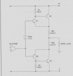
Christer,
and what I speak about is the attached topology.
Q1 and Q2 are quite important. Replacing R5 and R6 by current sources makes the parameters even better. After the replacement you have Jung's buffer with CFP output. This topology can be used not only for the power amp, but for the buffer, too. My requirement for buffer circuit is to handle 100 Ohm load (50 Ohm + 50 Ohm).
Pavel
Attachments
Hugh,
Just some quick notes.
For use in a diamond buffer for headphones or line level we will
typically be able to run in class A.
Although the figure from Slones book that I posted uses bipolars,
he does mostly/always use a BJT/MOSFET combo in his finished
designs in the book. He do run them in class AB, though. OTOH
he has obviously decided to go for ordinary source followers instead
in his newer OptiMOS design. He is a strong advocate for CFPs in
the book, so maybe ha has later changed his mind?
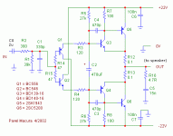
Regarding Hugh's comments, I do not hear this attributes for class A output stage as shown, the opposite seems to be true for class A operation of this stage. But I do strongly recommend to place this circuit inside the feedback loop (without input capacitor and without C1). The NFB will be closed around very linear class A output stage, reduces distortion even more and increases damping factor considerably to more than 1000 (8 Ohm) at lower frequencies and to 500 at 10kHz.
1
Hi Pavel, All,
(Compare above Pavel's circuit and previously attached/linked ones.)
Whereas there can be no clear line drawn, in my opinion there are two ways to view this topology. Two different roles for Q1/Q2.
a) a CFP output with a unusual Vbias generator (doubling as buffer for the VAS if this is part of standard amplifier).
b) a diamond buffer with aux power transistors to carry the most current.
And (still in speculation mode, and unusually subjective) whether this works more as a) or b) depends IMHO on matching between the Q1/Q2 and the Q3/Q4 pair.
If they are comparable in speed and other factors, the circuit has more the characteristics of b), otherwise it has more the characteristics of a). As I am mostly aiming towards b), I try a close match of Q1/Q2 and Q3/Q4.
But this of course gives some problems, if this has to be the output stage of power amplifier with 'real' currents to drive:
Either
1) Q1/Q2 and Q3/Q4 must have large bias currents, which 1a) rules out high beta devices or 1b) requires each of them to be a darlington
or
2) the booster transistors Q5/Q6 must be darlingtons.
Am I lost in Voodoo-land here or can somebody see sense in this argument?
Regards,
Peter Jacobi
Hi Pavel, All,
(Compare above Pavel's circuit and previously attached/linked ones.)
PMA said:[...]and what I speak about is the attached topology.
Q1 and Q2 are quite important. Replacing R5 and R6 by current sources makes the parameters even better. After the replacement you have Jung's buffer with CFP output.[...]
Whereas there can be no clear line drawn, in my opinion there are two ways to view this topology. Two different roles for Q1/Q2.
a) a CFP output with a unusual Vbias generator (doubling as buffer for the VAS if this is part of standard amplifier).
b) a diamond buffer with aux power transistors to carry the most current.
And (still in speculation mode, and unusually subjective) whether this works more as a) or b) depends IMHO on matching between the Q1/Q2 and the Q3/Q4 pair.
If they are comparable in speed and other factors, the circuit has more the characteristics of b), otherwise it has more the characteristics of a). As I am mostly aiming towards b), I try a close match of Q1/Q2 and Q3/Q4.
But this of course gives some problems, if this has to be the output stage of power amplifier with 'real' currents to drive:
Either
1) Q1/Q2 and Q3/Q4 must have large bias currents, which 1a) rules out high beta devices or 1b) requires each of them to be a darlington
or
2) the booster transistors Q5/Q6 must be darlingtons.
Am I lost in Voodoo-land here or can somebody see sense in this argument?
Regards,
Peter Jacobi
Christer,
Yes, I suspect you are right. Slone could well have changed his mind; instability is a problem in Class AB at the crossover disjunction; but of course in Class A this problem evaporates.
Pavel,
I concur with your findings in Class A. In fact, I use the bipolar/mosfet hybrid CFP in my Glass Harmony SE amp (which dissipates 3A/50V and produces just 28W) and its stability is unquestioned. In fact, its stability rivals QE2.
So, in summary, CFP is fine for Class A SE or PP, not so good for Class AB although it can be achieved at sonic cost with small caps across the base/collector of the driver. This is a great pity, as the CFP is very appealing from an engineering standpoint. There has been much crowing about the joy of a stable bias point, but in fact with just 1.3V I have found setting the bias to be almost a thermonuclear event, with outputs easily sacrificed to the silicon gods. Sonic and stability dictates show that the best overall results are still gained with the emitter/source follower, though my own preference will always be for Self's Type II double emitter follower.
Cheers,
Hugh
- Status
- This old topic is closed. If you want to reopen this topic, contact a moderator using the "Report Post" button.
- Home
- Amplifiers
- Headphone Systems
- Current feedback high speed headphone amp with diamond output buffer