Thanks Ryanj, ready for answer, like soldier on duty...Dady,
Ive got heaps of wire, have a read here: http://www.diyaudio.com/forums/swap...ameter-constantan-isotan-resistance-wire.html
Ryan
Best Regards
Isn't 200 mts of wire too much for the very weak current output signal of the DAC?, I'm not sure to test the honeycomb resistor.......
Dear Galeb,
Length of wire to use is desired R divided by the quoted R-per-meter of the resistance wire:
L= Rfinal/R-per-meter or
= Rfinal/Rwire/m
I use a 100 Ohm/m wire so it's 5m for a 500R honeycomb.
Cheers,
M.
If tubes offer advantages over semiconductors in a specific application I wouldn't hesitate to use them.
When I look at the latest schematics with the single mosfet I/V I can't help but wonder how this works better than a triode, I mean maybe a generalization but Lynn Olsen was pretty adamant that linearity of a single active device was superior with a triode over a mosfet over a bjt. So when I see a single active device (mosfet) as the analog stage one can be fairly(?) confident that linearity/thd is not spectacular and that somehow a tube should do a better job..
For the TDA1541 DAC we need a maximum 25mV difference between the i-out pin and the a-ground pin as the music plays, in other words an analog stage that offers near zero input impedance but sits 0.7V above the a-ground pin does us little good. Also a heavy feedback analog stage that sits 0 mV through the audio band but jumps over 25mV with 1mhz does us no good at meeting the chip's specification either.
Its not surprising many find high impedance passive i/v or jfet input sonically satisfying because the non-linearity of running above spec compliance voltage is buried in the loss of bit depth but without the shocking RF crud. So I don't turn my nose at the gentleman who is liking his Aikido output stage.
It is possible to have a tube gain stage with better than -96dB thd+N (just look at the Impasse project) and I have always wondered what would be the result should the great transformer "black artists" out there put as much resources into designing a step-up transformer around an i-out DAC that has been put into lp cartridge step-up transformers, would the long quest for a great 16 bit dac analog stage been solved?
I also think galvanic isolation from the DAC is overlooked, we fret about it on the input side of the chip but how many dac's have a little bump at 60hz and loads of HF into the mhz after the even analog stage and filtering? Surely a single Mosfet can't be the best solution
 ?
? Now the issue is a mic stepup transformer is a poor substitute for what we really need as far as a transformer to bump up the i-out level prior to a tube gain stage. The similarities to dealing with an i-out dac signal to classic microphones and phono catridge can be deceptive. The i-out DAC is a poor current source with a low 1k-2k ohm output impedance, and a poor voltage source with high output impedance
. Meaning a transformer I think needs to be about 1:4 with the right amount of primary inductance and enough current drive left to drive the subsequent gain stage which needs to be very easy to drive.One could consider the whole open loop transimpedance bjt i/v stages popular here nearly 10 years ago as basically silicone step-up transformers with worse noise, linearity, and filtering.
You said earlier you gave up on step-up transformers for the TDA1541, but would you consider the possibility that the transformer designers "gave up" on i-out DAC's instead ?
Maybe instead of worrying about resistor winding we would be better to look at step-up transformer design ?
Last edited:
Here is my attempt of a combined step-up transformer tube I/V converter:
http://www.diyaudio.com/forums/digi...s-valve-output-stage-lundahl-transformer.html
I think better noise figures could be achieved - I used the simplest anode and filament supply for the tests, and no special consideration for the layout.
http://www.diyaudio.com/forums/digi...s-valve-output-stage-lundahl-transformer.html
I think better noise figures could be achieved - I used the simplest anode and filament supply for the tests, and no special consideration for the layout.
Here is my attempt of a combined step-up transformer tube I/V converter:
http://www.diyaudio.com/forums/digi...s-valve-output-stage-lundahl-transformer.html
I think better noise figures could be achieved - I used the simplest anode and filament supply for the tests, and no special consideration for the layout.
Thankyou I had seen that long ago when I was stuck on the PCM1704 and not really discovered the TDA1541, this is a very unique i/v stage that realy has a lot of advantages. Do you still use it, happy with it ? Any updates/reinfiements possibly could update the thread?
Hi regal,
The circuit is a common gate circuit or current buffer. Properties are unity current gain (i in = i out), low noise, large bandwidth (up to ft), high stability, low input impedance, high output impedance.
DC offset at the TDA1541A output can be nulled by the 250K trimmer in the schematic. Impact of exceeding DAC output compliance depends on the circuit that is used. Exceeding output compliance has biggest impact when using passive I/V resistor between DAC output and ground and lowest impact when driving a current buffer for example.
The current buffer circuit with 500 Ohm passive I/V resistor offers approx. 500 Ohm output impedance. THD measurements show low distortion and the high level of refinement in the sound indicates high bit resolution.
The world's best transformer can't challenge a DC coupling (short piece of wire). Step-up transformers are likely to have high output impedance and limited bandwidth.
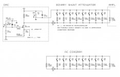
I use balanced power supplies that isolate the circuit from mains interference and minimizes ground loops. The DAC output is isolated from the 500 Ohm passive I/V resistor using a grounded gate buffer. The 500 Ohm passive I/V resistor is also part of a binary stepped shunt volume control. So I basically vary I/V resistor value by shunting it.
Microphones and cartridges generate continuous analogue signals. DACs generate RF signals that consist of subsequent pulses (samples). Two completely different signals that require completely different signal processing.
Step up transformers do not perform I/V conversion so I/V resistor would still be required and resistor properties would still be critical.
When I look at the latest schematics with the single mosfet I/V I can't help but wonder how this works better than a triode, I mean maybe a generalization but Lynn Olsen was pretty adamant that linearity of a single active device was superior with a triode over a mosfet over a bjt. So when I see a single active device (mosfet) as the analog stage one can be fairly(?) confident that linearity/thd is not spectacular and that somehow a tube should do a better job..
The circuit is a common gate circuit or current buffer. Properties are unity current gain (i in = i out), low noise, large bandwidth (up to ft), high stability, low input impedance, high output impedance.
For the TDA1541 DAC we need a maximum 25mV difference between the i-out pin and the a-ground pin as the music plays, in other words an analog stage that offers near zero input impedance but sits 0.7V above the a-ground pin does us little good. Also a heavy feedback analog stage that sits 0 mV through the audio band but jumps over 25mV with 1mhz does us no good at meeting the chip's specification either
DC offset at the TDA1541A output can be nulled by the 250K trimmer in the schematic. Impact of exceeding DAC output compliance depends on the circuit that is used. Exceeding output compliance has biggest impact when using passive I/V resistor between DAC output and ground and lowest impact when driving a current buffer for example.
Its not surprising many find high impedance passive i/v or jfet input sonically satisfying because the non-linearity of running above spec compliance voltage is buried in the loss of bit depth but without the shocking RF crud. So I don't turn my nose at the gentleman who is liking his Aikido output stage.
The current buffer circuit with 500 Ohm passive I/V resistor offers approx. 500 Ohm output impedance. THD measurements show low distortion and the high level of refinement in the sound indicates high bit resolution.
It is possible to have a tube gain stage with better than -96dB thd+N (just look at the Impasse project) and I have always wondered what would be the result should the great transformer "black artists" out there put as much resources into designing a step-up transformer around an i-out DAC that has been put into lp cartridge step-up transformers, would the long quest for a great 16 bit dac analog stage been solved?
The world's best transformer can't challenge a DC coupling (short piece of wire). Step-up transformers are likely to have high output impedance and limited bandwidth.
I also think galvanic isolation from the DAC is overlooked, we fret about it on the input side of the chip but how many dac's have a little bump at 60hz and loads of HF into the mhz after the even analog stage and filtering? Surely a single Mosfet can't be the best solution?
I use balanced power supplies that isolate the circuit from mains interference and minimizes ground loops. The DAC output is isolated from the 500 Ohm passive I/V resistor using a grounded gate buffer. The 500 Ohm passive I/V resistor is also part of a binary stepped shunt volume control. So I basically vary I/V resistor value by shunting it.
Now the issue is a mic stepup transformer is a poor substitute for what we really need as far as a transformer to bump up the i-out level prior to a tube gain stage. The similarities to dealing with an i-out dac signal to classic microphones and phono catridge can be deceptive. The i-out DAC is a poor current source with a low 1k-2k ohm output impedance, and a poor voltage source with high output impedance. Meaning a transformer I think needs to be about 1:4 with the right amount of primary inductance and enough current drive left to drive the subsequent gain stage which needs to be very easy to drive.
Microphones and cartridges generate continuous analogue signals. DACs generate RF signals that consist of subsequent pulses (samples). Two completely different signals that require completely different signal processing.
Maybe instead of worrying about resistor winding we would be better to look at step-up transformer design ?
Step up transformers do not perform I/V conversion so I/V resistor would still be required and resistor properties would still be critical.
Hi marconi118,
I attached a schematic.
In the MK9 I am experimenting with different JFETs and MOSFETs, JFETs require negative bias voltage, MOSFETs positive bias voltage.
The effects of TDA1541A output compliance on output signal THD depends on the application.
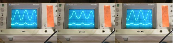
Second picture shows oscillograms of the JFET current buffer.
Oscillograms show effect of varying DC level on DAC output. With this circuit I can vary DC level by changing JFET gate voltage (source voltage then "follows").
Upper channel shows output signal (using 1 : 10 probe).
Lower channel shows signal at the TDA1541A output ( using 1 : 10 probe).
Measured distortion is lowest @ -150mV with this application.
FET current buffer input impedance has limits (20 ... 50 Ohms). The impedance alo changes with drain current (impedance increases with decreasing drain current).
This explains the peak signal @ 500mVpp (iD = 0) and lowest level when iD = 4mA.
Adding a constant bias current reduces ac voltage at the TDA1541A output, but (RF) power supply noise and CCS equilibrium noise will mask LSBs. This only works when using a CCS with at least 100 MHz bandwidth, impedance greater than 2 M Ohm over this entire bandwidth and very low thermal drift.
The signal shape at the TDA1541A output pin can be explained by the fact that FET current buffers have certain impedance (20 ... 50 Ohm typical) and that gain reduces with drain current. So the peak signal occurs when TDA1541A output current approaches / equals zero (lowest gain).
The 500 Ohm passive I/V resistor is also part of a binary stepped shunt volume control. So I basically vary I/V resistor value by shunting it.
Hello, could you please post a principle schematics of this?
I attached a schematic.
In the MK9 I am experimenting with different JFETs and MOSFETs, JFETs require negative bias voltage, MOSFETs positive bias voltage.
The effects of TDA1541A output compliance on output signal THD depends on the application.
Second picture shows oscillograms of the JFET current buffer.
Oscillograms show effect of varying DC level on DAC output. With this circuit I can vary DC level by changing JFET gate voltage (source voltage then "follows").
Upper channel shows output signal (using 1 : 10 probe).
Lower channel shows signal at the TDA1541A output ( using 1 : 10 probe).
Measured distortion is lowest @ -150mV with this application.
FET current buffer input impedance has limits (20 ... 50 Ohms). The impedance alo changes with drain current (impedance increases with decreasing drain current).
This explains the peak signal @ 500mVpp (iD = 0) and lowest level when iD = 4mA.
Adding a constant bias current reduces ac voltage at the TDA1541A output, but (RF) power supply noise and CCS equilibrium noise will mask LSBs. This only works when using a CCS with at least 100 MHz bandwidth, impedance greater than 2 M Ohm over this entire bandwidth and very low thermal drift.
The signal shape at the TDA1541A output pin can be explained by the fact that FET current buffers have certain impedance (20 ... 50 Ohm typical) and that gain reduces with drain current. So the peak signal occurs when TDA1541A output current approaches / equals zero (lowest gain).
Attachments
In the MK9 I am experimenting with different JFETs and MOSFETs, JFETs require negative bias voltage, MOSFETs positive bias voltage.
The effects of TDA1541A output compliance on output signal THD depends on the application.
Second picture shows oscillograms of the JFET current buffer.
Oscillograms show effect of varying DC level on DAC output. With this circuit I can vary DC level by changing JFET gate voltage (source voltage then "follows").
Good. Now we need a current buffer fot the output of the humble TDA1543...I don't remember seing any...
As it has only positive supply, I imagine Mosfet would be ideal...Thanks.
M.
Hi maxlorenz,
TDA1543 output circuit is different from TDA1541A and needs no current buffer.
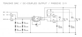
I attached schematic of a TDA1543 DAC with DC-coupled outputs and passive I/V conversion.
This is the best performing (and easiest to build) TDA1543 circuit I designed so far (tested on MK9 prototype setup with latest timing module).
R1, R2, D1 ... D6 are WS / DATA limiters (1.8Vpp).
C1 is a 1uF 1210 SMD film cap soldered directly to TDA1543 pins 4 and 5 as close to the plastic housing as possible.
R3 and R4 are passive I/V resistors that offer approx. 0.0025 * 820 = 2.05Vpp output signal.
P1 is passive I/V resistor bias voltage (adjust to 3.2V).
P2 provides DC-coupled outputs (no coupling cap required). Adjust P2 for lowest DC offset on R and L outputs. This would give around 2.2V on the wiper of P2.
TDA1543 requires a super clean 5V power supply (balanced or battery power supply) and ultra low jitter BCK signal with white noise residual jitter spectrum.
Good. Now we need a current buffer fot the output of the humble TDA1543...I don't remember seing any... As it has only positive supply, I imagine Mosfet would be ideal...
TDA1543 output circuit is different from TDA1541A and needs no current buffer.
I attached schematic of a TDA1543 DAC with DC-coupled outputs and passive I/V conversion.
This is the best performing (and easiest to build) TDA1543 circuit I designed so far (tested on MK9 prototype setup with latest timing module).
R1, R2, D1 ... D6 are WS / DATA limiters (1.8Vpp).
C1 is a 1uF 1210 SMD film cap soldered directly to TDA1543 pins 4 and 5 as close to the plastic housing as possible.
R3 and R4 are passive I/V resistors that offer approx. 0.0025 * 820 = 2.05Vpp output signal.
P1 is passive I/V resistor bias voltage (adjust to 3.2V).
P2 provides DC-coupled outputs (no coupling cap required). Adjust P2 for lowest DC offset on R and L outputs. This would give around 2.2V on the wiper of P2.
TDA1543 requires a super clean 5V power supply (balanced or battery power supply) and ultra low jitter BCK signal with white noise residual jitter spectrum.
Attachments
Last edited:
TDA1543 output circuit is different from TDA1541A and needs no current buffer.
I attached schematic of a TDA1543 DAC with DC-coupled outputs and passive I/V conversion.
Thank you!
I had also that idea of soldering directly the cap to the power and G pins.
Very interesting concept. I shall try it soon.
Hi Dr.H,
The TDA1543 is powered by the +5V TDA1541A supply. This consists of a balanced capacitance multiplier followed by a balanced filtered-buffered zener regulator.
I use slaved integrated source (SD-transport). This eliminates S/PDIF and USB source issues alltogether. So I "only" have to focus on masterclock and connected circuit properties.
By integrating CCS / shunt voltage regulator, masterclock, sine to square conversion and division on a miniature timing module (12mm x 35mm x 5mm) it is easier to maintain reproducible extreme low jitter and residual jitter spectrum.
ECDesigns, what power supply do you feed the 1543? Also, how do you get ultra low jitter BCK signal with white noise residual jitter spectrum?
The TDA1543 is powered by the +5V TDA1541A supply. This consists of a balanced capacitance multiplier followed by a balanced filtered-buffered zener regulator.
I use slaved integrated source (SD-transport). This eliminates S/PDIF and USB source issues alltogether. So I "only" have to focus on masterclock and connected circuit properties.
By integrating CCS / shunt voltage regulator, masterclock, sine to square conversion and division on a miniature timing module (12mm x 35mm x 5mm) it is easier to maintain reproducible extreme low jitter and residual jitter spectrum.
Thanks ecdesigns, you've bee a generous fount of knowledge!
I'm keen to build a couple of your balanced designs as per schematics you've posted earlier. Will report here, juts have to find the time...
I've slaved a PCM63 based to a "Shigaclone" and liked the result-sharper images, lower noise floor.
How would one slave a CS8412-1543 NOS dac to a transport?
I'm keen to build a couple of your balanced designs as per schematics you've posted earlier. Will report here, juts have to find the time...
I've slaved a PCM63 based to a "Shigaclone" and liked the result-sharper images, lower noise floor.
How would one slave a CS8412-1543 NOS dac to a transport?
Hi Dr.H
If I am correct the Shigaclone only outputs S/PDIF. This signal is derived from the Sanyo LC78601 chip (pin 29). So one is stuck with S/PDIF only.
I suggest to use a Wolfson WM8804 receiver with external crystal, this one for example:
The S/PDIF Transceiver Module
CS8412 isn't really a good S/PDIF receiver chip with 200ps rms typical PLL clock jitter plus interlink plus source jitter.
WM8804 datasheet indicates typical 50ps rms PLL jitter. If I am correct source jitter is attenuated by means of reclocking with an on-chip crystal oscillator.
TDA1543 uses BCK for sample timing, so this signal needs to have low jitter.
If I am correct the shigaclone masterclock equals 16.9344 MHz.
You could remove crystal and both caps close to it and get a 16.9344 MHz low jitter masterclock (Tent Labs for example) and place it in the DAC.
Now buffer the masterclock output and feed it to the crystal pad that connects to LC78601 chip pin 61 (X-in).
BCK (2.1168 MHz) can now be derived straight from the masterclock using a synchronous divide by 8 circuit.
I've slaved a PCM63 based to a "Shigaclone" and liked the result-sharper images, lower noise floor.
How would one slave a CS8412-1543 NOS dac to a transport?
If I am correct the Shigaclone only outputs S/PDIF. This signal is derived from the Sanyo LC78601 chip (pin 29). So one is stuck with S/PDIF only.
I suggest to use a Wolfson WM8804 receiver with external crystal, this one for example:
The S/PDIF Transceiver Module
CS8412 isn't really a good S/PDIF receiver chip with 200ps rms typical PLL clock jitter plus interlink plus source jitter.
WM8804 datasheet indicates typical 50ps rms PLL jitter. If I am correct source jitter is attenuated by means of reclocking with an on-chip crystal oscillator.
TDA1543 uses BCK for sample timing, so this signal needs to have low jitter.
If I am correct the shigaclone masterclock equals 16.9344 MHz.
You could remove crystal and both caps close to it and get a 16.9344 MHz low jitter masterclock (Tent Labs for example) and place it in the DAC.
Now buffer the masterclock output and feed it to the crystal pad that connects to LC78601 chip pin 61 (X-in).
BCK (2.1168 MHz) can now be derived straight from the masterclock using a synchronous divide by 8 circuit.
- Home
- Source & Line
- Digital Line Level
- Building the ultimate NOS DAC using TDA1541A