Gootee, is this what you mean for the C1, C2 caps?
It's done in Eagle, and I can post the files here if the layout is ok.
The ones I was looking at are now labeled C5 and C6. They are the 0.1 uF bypass/decoupling capacitors for the chip's power pins. They are now better than before but should actually still be pushed a little closer (both could be moved to the right, on your latest layout).
Last edited:
The ones I was looking at are now labeled C5 and C6. They are the 0.1 uF bypass/decoupling capacitors for the chip's power pins. They are now better than before but should actually still be pushed a little closer (both could be moved to the right, on your latest layout).
That's because I am a different person than the original poster
")
I was hoping to illustrate your point with a pic of a layout which I did.
For the OPs benefit, I am posting the eagle files, incorporating
the suggestions.
Notes:
1) SGND and PGND points are brought out separately.
2) If you need external mute, do not populate Rm1.
3) Verify and use at your own risk.
Attachments
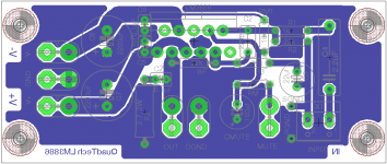
1. Isn't there clearance UNDER the chip so that the V-'s 0.1 uF bypass cap could connect right next to the pin? Might have to thin the power trace a little in order to extend a small ground trace around the back of the chip pads. A 0.1 uF X7R ceramic capacitor would work best there, probably, and they are extremely small (like 0.2" LS (lead spacing), 0.2" L x 0.2" H x 0.125" W).
2. If the two 0.1 uF caps got pushed under the chip or between its pins, then the two 2200 uF caps could be moved closer. Just make sure that there is SOME clearance between them and the chip and heatsink, since heat is bad for electrolytics.
3. Connect the Zobel cap RIGHT AT the chip pin.
4. The 220p cap and the 880 (?) R (R3) need to go to the left as much as possible, closer to the pins. The 220p could also angle toward the rear pin. Then the 10K could also go left and be angled similarly, and the 1K and 22K could go left to connect closer to the input pin. Wait. Scratch that. ACTUALLY, it looks like the 10K should just go behind the back row of pins. Then maybe you could pull R1 and R2 way in and run the cmute trace around the outside (rear) of the 220p and under R1 and R2! And in that case, a 220p NPO ceramic should fit directly against the input pins, under the chip. Then the input resistors can come all the way in. Now we're getting somewhere! [Resistors for amplifier input pins (especially the negative input) should always be connected right AT the pin, if possible, so there's as little stray inductance as possible. Ditto for the bypass caps at the power pins.]
5. Need to fill in to remove all acute angles, such as around pads. Some appear to be "tangentiallly" connected. Fill the gaps. They are "etchant traps".
6. Remove the copper from the drill holes, if possible.
7. Should the rear face of the chip be right at the rear edge of the board, for easiest heatsink attachment?
8. Suggest extending traces (same width as pads) from input cap pads toward each other, in case someone needs to drill for different lead-spacing.
Last edited:
The signal input ground reference point should be run separately (i.e. with a separate wire), all the way back to the star ground on the main power supply board (probably between the main smoothing cap ground connections?).
The signal input and signal input ground-return traces (and wiring) should stay absolutely as close together as possible, everywhere. I would go to the trouble of changing the ones near the input cap, so that they are right against each other, with a minimum gap between them, for absolutely as much of their length as possible, right up to the input-to-ground resistor. No need to let the capacitor width determine the distance between the traces. Maybe even put the cap OVER the ground-return trace. [The idea is to have zero "enclosed loop area", in order to not have any currents induced in the loop by time-varying magnetic or electromagnetic fields in the air, which can be a major and common source of power supply hum (not to mention RFI). See "Faraday's Law".]
You might also want to leave space for a resistor and parallel inductor in series with the output.
Last edited:
You MIGHT want to also have a separate isolated ground return for the output Zobel network.
I'm not sure about the Mute circuit's ground return but I suspect that it would be much better to connect it with the isolated input ground reference for its connection back to the power supply than to lump it in with the output ground. Either do that or run it completely separately.
I'm not sure about the Mute circuit's ground return but I suspect that it would be much better to connect it with the isolated input ground reference for its connection back to the power supply than to lump it in with the output ground. Either do that or run it completely separately.
Last edited:
......... Look at PIN2. It is not connected. You can use this spare PCB area to thicken traces.....................
............................you may find that very small ceramic caps make for excellent power pin decoupling. These can be fitted much closer to the Power PINs than those big 0.2" pin pitch film caps shown.
C1 and C2 are too far from the chip's pins. ..................
........... They are the 0.1 uF bypass/decoupling capacitors for the chip's power pins. They are now better than before but should actually still be pushed a little closer (both could be moved to the right, on your latest layout).
you are being told repeatedly that HF decoupling must be moved closer !!!!1. Isn't there clearance UNDER the chip so that the V-'s 0.1 uF bypass cap could connect right next to the pin? Might have to thin the power trace a little in order to extend a small ground trace around the back of the chip pads. A 0.1 uF X7R ceramic capacitor would work best there, probably, and they are extremely small (like 0.2" LS (lead spacing), 0.2" L x 0.2" H x 0.125" W).
2. If the two 0.1 uF caps got pushed under the chip or between its pins, then the two 2200 uF caps could be moved closer. Just make sure that there is SOME clearance between them and the chip and heatsink, since heat is bad for electrolytics.
Hi,
I think decoupling is close enough. Also, small caps in parallel with low ESR caps can cause resonance with corresponding high impedance peaks at high frequency. It's recommended to use standard electrolytic if paralleled with small low loss caps.
I am sorry but I must disagree with your "close enough" guess. On what do you base it? The inductance which is proportional to the length of the PCB trace between the pin and the bypass capacitor is a problem that needs to be mitigated. What length would you say would NOT be close enough and why? Anyway, accepted best practice is to make the distance as close to zero as possible and always less than 2 mm (and less for high-frequency circuits). So if that's easily-enough done then why not (especially when we're talking about a PCB design, which might be around for a long time and might be used by many)?
Yes, you make a good point, that a small cap can form a resonance when paralleled with a larger cap. But that's due to the _inductance_ of the larger cap and the small capacitance (combined with the inductance presented by the PCB traces, et al) forming an LC resonance, which can be a problem if there is too little damping (capacitor ESR). But lower ESR makes a better bypass or decoupling cap. And the 2200 uF caps could use low ESR, maybe especially at low frquencies where a "low ESR" rating is meaningful. That's one of the reasons why I suggested using an X7R ceramic for the 0.1 uF, and not a film cap or an NPO ceramic.
ESR of electrolytic caps varies significantly with frequency. At high frequencies (where the resonance would be), basically _every_ large electrolytic capacitor (not just "low ESR" types) will have a very low ESR. So a small cap that is paralleled with a relatively-large electrolytic should basically never be a "low loss" type, such as film or NPO/C0G ceramic, unless one is a very careful and sophisticated designer, or, knows how to design an optimal snubber resistance and add the proper series capacitance value to it to prevent excessive dissipation.
I am sorry but I must disagree with your "close enough" guess. On what do you base it?
Hi gootee,
Do we discuss the same layout? Decoupling is in fact very close.
Well, first of all, the data sheet for 3886 does not mention any requirement that decoupling must be placed right at the pins. However, the datasheet does recommend that decoupling should be placed as close as possible next to the chip. I do think that proper decoupling is well addressed in the latest layout shown at this page. Where do we draw the line?
Ther is a whole wealth of information regarding de-coupling on the web, it is a critical part of any electronic design these days, as there is more and more high frequency noise being created, both airborne and mains borne, never mind the digital devices and components in most peoples systems.
Such info as Analog Devices MT-101, first one I picked up on my desk.
For high frequency de-coupling it is the parasitic inductance that is the killer, so the smaller the route between pin and cap the better. Also small package X7R or COG MLCC caps (SMD 0603's 0402's) are best for this due to LOW parasitic inductance.
As to where do we draw the line, well the big 3 proffesional packages (Mentor, Zuken and Cadence) all now offer power delivery system integrity software.
This was yatgai's topic, but in view of the feedback given
to my layout, I incorporated them and will post once more here,
with due apologies to the OP.
to my layout, I incorporated them and will post once more here,
with due apologies to the OP.
An externally hosted image should be here but it was not working when we last tested it.
Attachments
Hi.
Would it not be good practise to take the speaker out 0 volt from directly inbetween C7 and C8. Im assuming that C5 and C6 also the 220pF across the input pins are to be soldered underneath the board. have a look at this link. From the menu select bypassing . Tutorials, Electronics made EASY, Williamson Labs
Regards
Ian
Pretty good work, so far! But those vertical resistors should be turned around so that the excess lead length is not connected to the chip pins.
And I would still want the input signal ground to run right next to the input signal trace(s), everywhere possible, removing the little board-ground stub from between them and right-angling one of them to be next to the other starting directly at the input connector, and putting stubs out to get to those electrolytic caps if necessary. The input traces are critical, since they are a low-level signal which will be amplified. Any geometric area between them will amount to more hum and RF in the input signal.
And I think I agree with all of what madtecchy said is needed, just above. Perhaps a jumper wire would be needed from an isolated output ground to between the two large caps. C5 and C6 could just be pushed a little closer to the pins, though. And the 220 pF should be pulled down to have its pads touch both input pins' pads. I have tried it with my PCB software and it can fit there.
Last edited:
Thanks! I'll make the suggested changes (as best as I can ).
Madtecchy - yes, I did plan to solder the bypass caps on
the copper side - can't get closer than that. I may just add pads
for SMD bypass caps too, for max flexibility.
I appreciate the suggestions and handholding towards
a good layout.
Anyone wanting the latest eagle files, pls PM me.
).Madtecchy - yes, I did plan to solder the bypass caps on
the copper side - can't get closer than that. I may just add pads
for SMD bypass caps too, for max flexibility.
I appreciate the suggestions and handholding towards
a good layout.
Anyone wanting the latest eagle files, pls PM me.
Hi Quadtec.
I totaly agree with the S.M.D pads for the decoupling capacitors. Im guessing you will be building this amplifier very soon. Then you can start changing components im amazed by the diffrence components from diffrent manufacturers can influence the sound of these great sounding I.C's. Have fun there is much to be learned from building this type of amplifier and it will put you in good stead to take on more complex discrete Designs. Ps the link i posted was kindley given to me by gootee so thanks is due .Thankyou gootee
Kind Regards
ian
According to my interpretation of Henry Ott, you will want to connect the four decoupling capacitors all to the load ground pin as directly as possible.
If you don't want to re-work the entire layout, you should consider adding a very thick short wire, from right behind the chip's load ground pin to a point near the ground end of C6. And if you do that, then I guess you might as well isolate the ground area containing the output ground pin and output ground connector from the rest of the board-ground copper.
P.S. Don't forget to also fill in all of the little gaps between pads and copper, and eliminate all of the acute angles in the copper, including pads-to-copper and copper-to-copper (no angles should be 90 degrees or less).
According to my interpretation of Henry Ott, you will want to connect the four decoupling capacitors all to the load ground pin as directly as possible.
If you don't want to re-work the entire layout, you should consider adding a very thick short wire, from right behind the chip's load ground pin to a point near the ground end of C6. And if you do that, then I guess you might as well isolate the ground area containing the output ground pin and output ground connector from the rest of the board-ground copper.
P.S. Don't forget to also fill in all of the little gaps between pads and copper, and eliminate all of the acute angles in the copper, including pads-to-copper and copper-to-copper (no angles should be 90 degrees or less).
(Note that madtecchy suggested the above, in post 33. Good call.)
I seems like C5 and C6 (the 0.1uF decoupling caps) should be able to go between the rows of chip pins, and connect the power pins almost directly to the output ground pin. They could probably just be soldered to the pins themselves, or maybe even just have their leads inserted into the same holes as the chip pins. But they should also be able to fit with their own pads, especially the really-small types that are available. The surface mount idea would work great too, of course.
It would probably be a good idea to also keep in place some 0.1uF caps where they are currently shown.
Last edited:
possibly rather than probably. One must check for resonance, if adopting two capsIt would probably be a good idea to also keep in place some 0.1uF caps where they are currently shown.
I could recommend you a design I have built myself. It has probably no noise (cant hear any if sealed in metal box). CIRCUIT.lt : Elektronikos projektai The problem is that it is in Lithuanian. If you look in end of the article you can see that you can download pcb. Beware that pcb is mirrored (if you want unmirrored you should rotate so you can see CIRCUIT.LT). Just google translate it. If you need any help, PM me. Good luck!
- Status
- This old topic is closed. If you want to reopen this topic, contact a moderator using the "Report Post" button.
- Home
- Amplifiers
- Chip Amps
- Help on LM3886 PCB Routing