The output impedance of the D/A chip is also an interesting matter, it should have an inductive characteristic like most amplifier outputs, right? The impedance will rise with frequency.
My question is, if we put a capacitive load, will there be resonance/oscillations at some high frequency?
(This is interesting stuff, for me it´s more about learning than about seeking perfect audio. Altough it´s nice when you hear an improvement") )
)
-Alex
My question is, if we put a capacitive load, will there be resonance/oscillations at some high frequency?
(This is interesting stuff, for me it´s more about learning than about seeking perfect audio. Altough it´s nice when you hear an improvement
)-Alex
Op-amps aren't all that bad, yaknow.
The circuit is ingenious and I like its simplicity. Yet I somewhat disagree with the author's dislike of op-amps. The oscillation and stability issues are methinks well known and understood in the analog design circles, any good analog design book will talk about those at length. Say Bob Pease's Troubleshooting Analog Circuits. The distortion is surprisingly good for such a simple circuit, yet can be beat fairly easily with a good single op-amp design. Just off the top of my head, an LT1468 with a couple dozen pF between output and negative input will easily outdo this circuit's distortion when fed from a decent current-output DAC. It may end up costing the same, as good quality discretes for the jfet circuit aren't free, and it's obviously perhaps much less fun to "just slap an op-amp", but one can't say the performance can't be matched and beat with op-amps.
The thing about op-amps in such applications, though, is that it's much harder to prototype. You absolutely need to put stuff directly on the ground plane -- say dead bug technique. Leaded local decoupling capacitors should be promptly forgotten about; an 0805 or 0603 directly between the pin and ground is a must. It's a shame that rdi-wainwright is now defunct. They sold the german solder-mount (a.k.a. mini-mount) prototyping boards, and those were perfect for high frequency design -- as shown in RAP's RAQ on prototyping.
Almost any op-amp that will provide over 16 bits of performance at audio bandwidths will have gain-bandwidth products in 100+MHz range, with at least tens of V/us of slew rate. It really needs to be treated like an RF part. That's perhaps a drawback of op-amps -- yes, the circuit may have bandpass in the audio range only, but it needs all the tricks from RF or fast digital designer's handbook.
I personally can't fathom designing anything that should have good performance in the audio range without very carefully measuring the prototype using RF techniques. For high impedance nodes I use 500MHz FET probes with coaxial connection directly to a coaxial test socket on the prototype, and Tek 7104 scope with 50Ohm input plugin or 7934 and 7A13, perhaps with an extra preamp on the input. For low impedance nodes, I try to accommodate a short hardline going directly to the input of the preamp in front of the scope or analyzer.
I like to bang various nodes with a fast pulser to see if it recovers quietly, and make sure it can't be gotten into oscillation. I use a spectrum analyzer to make sure that wideband hash (100MHz bandwidth at a minimum) injected into power supplies doesn't disturb things -- again, "low frequency" sections are isolated from each other and from PS input with chokes/beads, and there are shunt supply "cleaners" a-la Pease's ripple rejection stuff and Salas's "simplistic" shunt, although they have to work up to 50MHz or so, and that's a whole different ballgame. Those circuits are notoriously hard to simulate without doing a FEM electromagnetic modeling first to extract all the parasitics from the circuit. Since the software for that runs into $10ks and you still need to prototype, one may as well start with a prototype and keep going until it performs well (may well be a dozen prototypes later). That's what I do, at least. YMMV.
I don't do audio, but I do instrumentation where I need high-end audio-like performance -- THD+N below -100dB in a 20kHz bandwidth around the carrier. Many of the circuits I do are pretty much unachievable with through-hole components. Yes, you can do 1GHz preamps with through-hole discretes here and there, but one ends up spending inordinate amounts of time tweaking and trimming the circuit to get a good response. SMT for everything but bulk decoupling caps is what I do, and I can't complain. Of course tools needed for the job start adding up -- a hot plate and hot air rework tool, stereo scope, etc -- you can do through-hole assembly and rework with a fraction of that, for sure.
Yeah, it perhaps was a long-ish rant, but I'm new here
The circuit is ingenious and I like its simplicity. Yet I somewhat disagree with the author's dislike of op-amps. The oscillation and stability issues are methinks well known and understood in the analog design circles, any good analog design book will talk about those at length.
It's not an issue of oscillation and stability so much as the fact that the
op amp is required to process a lot of high frequency noise as well as
signal. My experience is that an open loop fet can swallow the noise up
with aplomb, but even good op amps exhibit artifacts.
That aside, this is DIY audio, and the more DIY the better, so I give
preference to discretes wherever practical.
1:1 ratio transfo is apparently a stupid idea, it doesn't change anything.
But can it erase in part the digital noise?
Audio Note use them in their dac after the D/A chip, but I don't understand exactly why.
I think there are step-up transfos, but what are the pros and cons...?
Is anybody out there?
But can it erase in part the digital noise?
Audio Note use them in their dac after the D/A chip, but I don't understand exactly why.
I think there are step-up transfos, but what are the pros and cons...?
Is anybody out there?
Great, thanks! Very elegant and simple. I do have two questions you might be able to help me with.
1. Would it be an improvement to have a capacitor on the "wiper" pin to gnd?
2. Could the jfet gates be connected to the reference pin on the dac chip instead of the pot? (I don't know the ESS that well, but many TI chips have a reference pin)
1. Would it be an improvement to have a capacitor on the "wiper" pin to gnd?
2. Could the jfet gates be connected to the reference pin on the dac chip instead of the pot? (I don't know the ESS that well, but many TI chips have a reference pin)
1. Would it be an improvement to have a capacitor on the "wiper" pin to gnd? 2. Could the jfet gates be connected to the reference pin on the dac chip instead of the pot? (I don't know the ESS that well, but many TI chips have a reference pin)
1) You would likely want some resistance in series with such a cap to
prevent parasitic oscillation, so you can just use the pot for that.
2) If you want the Sources to be at the voltage of the reference pin, and
the fets are adequately matched, don't see any reason you couldn't.
Keep in mind that the reference pin may or may not be as quiet as you
want, so RC filtering might be appropriate.
Hope Nelson would forgive me for advertising for Jan Didden.
I wrote an article for Jan's Linear Audio (Volume 2) in June titled "Zen->Cen->Sen IV".
It made some interesting comparison between 3 minialisitic IV designs, all based on a pair of matched JFETs and a few components.
Both in simulation and hardware.
I shall open a new thread at the digital forum to show some details and pictures after the Volume 2 is open for order.
Should be some time next week.
Patrick
PS
Correction -- it is already open to order now at http://www.linearaudio.net/.
I shall post later today.
And yes, Jan has my admiration and support for devoting his time and finance after retirement to publish "Linear Audio".
For our benefit rather than his.
.
Last edited:
Posted here :
http://www.diyaudio.com/forums/digi...-sen-evolution-minimalistic-iv-converter.html
Patrick
http://www.diyaudio.com/forums/digi...-sen-evolution-minimalistic-iv-converter.html
Patrick
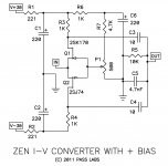
Interesting discrete circuit for an I/V converter.
However, I cannot help but wonder: what is the linearity of this circuit ?
A high end 24 bits DAC has a very high linearity. If this I/V converter has worse linearity than the DAC, the resulting linearity will be correspondingly worse.
In other words, the I/V converter has a very hard task ahead, otherwise it is the weakest link in the channel.
Is this circuit up to this task ?
Excellent question. Would SPICE simulation be able to provide an answer? I've used simplified current output models for high-speed DACs to aid in simulation of the I/V converter (using op-amps), so I assume that the FET/JFET version could be simulated as well. It's tough to find a SPICE model of the entire DAC, but sometimes you can do well enough with just the current output circuit, including any parasitic capacitance on the outputs.what is the linearity of this circuit ?
A high end 24 bits DAC has a very high linearity. If this I/V converter has worse linearity than the DAC, the resulting linearity will be correspondingly worse.
In other words, the I/V converter has a very hard task ahead, otherwise it is the weakest link in the channel.
Is this circuit up to this task ?
arround the three I/V (I/U) converter topologies about
http://www.passdiy.com/pdf/Z-IV.pdf
there are a wide range of posts, and I am not able to read them all.
I have heard only various op amps like OPA637, AD829 and OPA827 against a normal resistor with follow high input impedance line amp so as the D1-topology. From my view the D1 topology sounds at best, follow from the "only one resistor" topology about
http://www.dddac.de/pcm63/DAC_I-V_Resistor.htm
I/U converter that used op amps like the above mentioned still sound "over analytic" and a bit harsh like a tart wine.
The topology with jFETs so as various other discrete op amp solutions I have never heard.
Where can I find a description about the perceived audible differences between this various topologies?
Is there an I/U topology in the meantime, that beats clearly the D1 I/U converter ?
Last edited:
Where can I find a description about the perceived audible differences between this various topologies?
Is there an I/U topology in the meantime, that beats clearly the D1 I/U converter ?
on my web site: by-rutgers.nl
- Home
- Amplifiers
- Pass Labs
- Zen I/V Converter