I've uploaded a small article about an old but somewhat forgotten technique of distortion reduction applied to a single-ended FET amplifiers (could be used with valves too).
http://www.ant-audio.co.uk/Theory/Application_of_Indirect_Negative_Feedback.pdf
Perhaps Nelson will make another ZEN") ? That approach can be used in many applications. I attach a picture from the article with a (somewhat) simplified circuit.
? That approach can be used in many applications. I attach a picture from the article with a (somewhat) simplified circuit.
Cheers
Alex
http://www.ant-audio.co.uk/Theory/Application_of_Indirect_Negative_Feedback.pdf
Perhaps Nelson will make another ZEN
? That approach can be used in many applications. I attach a picture from the article with a (somewhat) simplified circuit.Cheers
Alex
Attachments
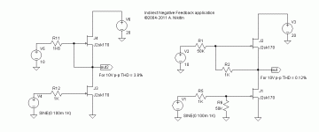
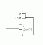
Looks like the upper FET is run in
Shunt Regulated Push Pull, SRPP
This is used with Tubeamplifiers.
The second harmonic is very suppressed giving lower overall THD
It would be good to see some examples. However with the indirect NFB all distortion components may be reduced, not just the second harmonic.
Cheers
Alex
The effect is so marginal it looks practically worthless.
Are there actual circuits where it would be of some value?
Try it at least with 2SK170 . The FETs you've used have very low gain without the feedback, so the effect is nil.
Cheers
Alex
Looks like the upper FET is run in
Shunt Regulated Push Pull, SRPP
This is used with Tubeamplifiers.
The second harmonic is very suppressed giving lower overall THD
It is not SRPP (where is the shunt?!) .
Cheers
Alex
Try it at least with 2SK170 . The FETs you've used have very low gain without the feedback, so the effect is nil.
Cheers
Alex
I guess the criteria are:
voltage gain factor of the FET >> gain with indirect feedback
transconductance of the FET times resistance of the two feedback resistors in series >> gain with indirect feedback
Is that correct?
By the way, I like the circuit. It is a variant of indirect feedback I hadn't seen before.
I guess the criteria are:
voltage gain factor of the FET >> gain with indirect feedback
transconductance of the FET times resistance of the two feedback resistors in series >> gain with indirect feedback
Is that correct?
Yes, you are absolutely correct.
By the way, I like the circuit. It is a variant of indirect feedback I hadn't seen before.
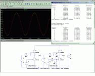
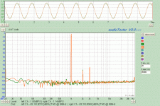
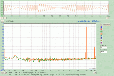
Thank you! I've designed this circuit about 7 years ago and used it with very good results. I won't give away exact circuits used in my commercial projects, however I can give you some ideas how a well polished circuit of this kind can work - by uploading a couple of graphs with spectrum of the output signal from a preamp built using that idea for the VAS. The gain is 20 dB (x10), the first graph is for the output voltage 1V RMS at 1 kHz, the second - for the output 0.5V RMS at 19+20kHz , both on 5 kOhm load.
Cheers
Alex
Attachments
Last edited:
Maybe I have missed something, but to me the first circuit looks like it has a drain load consisting of an FET wired as a CCS, in parallel with a 1k6 resistor. The second circuit has a slightly modified CCS in parallel with a 50K resistor. I would expect the first circuit to give high distortion. Nothing to do with indirect negative feedback, just a matter of changing the drain load for a triode-like device. Elvee gets much better results for the first circuit because he uses a much higher resistor value.
The 'explanation' also mentions identical FETs (OK in simulation, but where do you buy them?) and FETs whose drain current is independent of drain-source voltage (same question!). The second circuit might work OK, but not for the claimed reasons.
The 'explanation' also mentions identical FETs (OK in simulation, but where do you buy them?) and FETs whose drain current is independent of drain-source voltage (same question!). The second circuit might work OK, but not for the claimed reasons.
Maybe I have missed something, but to me the first circuit looks like it has a drain load consisting of an FET wired as a CCS, in parallel with a 1k6 resistor. The second circuit has a slightly modified CCS in parallel with a 50K resistor. I would expect the first circuit to give high distortion. Nothing to do with indirect negative feedback, just a matter of changing the drain load for a triode-like device. Elvee gets much better results for the first circuit because he uses a much higher resistor value.
The 'explanation' also mentions identical FETs (OK in simulation, but where do you buy them?) and FETs whose drain current is independent of drain-source voltage (same question!). The second circuit might work OK, but not for the claimed reasons.
You did miss something. The modulation of the input JFET drain current is exactly the same for both circuits, so is the gain. If your explanation was right, the gain in the second circuit should be 30 times higher, but it is not
. The trick is that in the second circuit the top FET is not just a current source any more, but rather a non-linear load which compensates for the non-linearity of the input FET. The indirect feedback loop takes care of that, making the resulting voltage transfer characteristic much more linear.Regarding the second point - for JFETs of the same type the transfer function for the same drain current would be identical enough for a good distortion compensation even when the devices are not matched perfectly (or at all) . The only problem would be a DC offset which would have to be corrected in either circuit by changing the bias voltage on V5 and V2 respectively.
And the third point -- even 2SK170 have enough voltage gain for this circuit to be useful and if required you can cascode two different JFETs in a usual manner - for example, as on the picture attached.
Cheers
Alex
Attachments
Last edited:
OK, I get it now. The first circuit has a CCS in parallel with 1k6. The second circuit has a modified source follower as load. Sorry.
I'm not sure whether this is feedback, feedforward or feed-alongside.
When I've designed this circuit in 2004 I had the same question and made some enquiries. The conclusion was that this is a case of what is called indirect feedback.
Cheers
Alex
When I've designed this circuit in 2004 I had the same question and made some enquiries. The conclusion was that this is a case of what is called indirect feedback.
Alex
I find some analogy between this your approach and Nelson's Aleph current source. You deal with jFETs and modulation on the basis of output voltage, Nelson with MOSFETs and modulation taken from the output current.
I was playing several years with the Aleph current source, making modulation weaker or stronger, and removing it at all. Measurement-wise, modulation always improve THD. However, soundwise, the best result (most live-like sound) was without modulation at all (suppose, due to effects of PS, which provides variable output signal current in the case with modulation). However, I am sure, the variants with modulation will sound better, if one would attach a relevant shunt power supply to this stage. However, this can have sense for preliminary stages only, not for output stage of power amp.
For me, your approach to linearisation immediately rises a question of a dedicated shunt PS for this stage. It is attractive to add modulated load to this my jFET schematics
http://www.diyaudio.com/forums/solid-state/197493-jfet-amp-current-nfb.html
However, first I should find out an amp, that will sound better than this schematics, at low wattage applications. Subjectively, from direct comparisons with transistor and SE and PP tube amps, and from indirect comparisons (sound memories from listenings of best brands in Singapore) I do not have motivation for further modifications. Maybe they could be important for commercial purposes, if I would obliged to report better THD.
Last edited:
Maybe I have missed something, but to me the first circuit looks like it has a drain load consisting of an FET wired as a CCS, in parallel with a 1k6 resistor. The second circuit has a slightly modified CCS in parallel with a 50K resistor. I would expect the first circuit to give high distortion. Nothing to do with indirect negative feedback, just a matter of changing the drain load for a triode-like device.
In fact, the appellation "indirect negative feedback" is misleading, even plain wrong in fact.
The circuit doesn't rely on NFB at all, it works by compensation.
The gain of an uncorrected stage is the ratio of the drain load resistance to the resistance created by 1/gfs, Rd*gfs.
But since gfs is non-linear, the gain and the transfer functions are non-linear.
If we replace the drain load by a similarly non-linear resistance, we can linearize the stage.
What we need is a load whose value is homothetic to 1/gfs, G*1/gfs: this creates a compensated gain=G.
The two resistors associated to the upper FET multiply the gfs by their ratio, and create the compensating impedance.
I see some practical problems though.
For the compensation to operate properly, it must not be disturbed by parasitic impedances => it can only work unloaded.
The 1/gfs multiplication will function with an idealized FET; with a real FET, the compensation will only be effective for G=1. With increasing values of G, the multiplied value will diverge from the optimum.
In fact, the compensation can only be perfect for G>1 if the devices are perfect. But of course, in this case, we can get rid of the compensation altogether, as it is not needed.
That the circuit doesn't rely on feedbak can be demonstrated easily.
Feedback will attenuate distortions, but also perturbating signals.
If a perturbating current is injected at the drain of both circuits, the resulting voltage will be similar. In raw amplitude, at least: in the second circuit, it will be distorted because of the non-linear load, but other than that they will be equal, for an equal gain.
In a stage utilizing feedback, the voltage would be further attenuated by the loop gain.
For given components, NFB would be more effective: the correction is agnostic, not selective and attenuates all non-linear effects, it utilizes the full raw gain available, and it is less sensitive to loading.
But the scheme should appeal to the the no-NFB brigade....
What do it happen when you apply a load ?
The load would reduce the open-loop gain and unbalance the currents, thus increasing the distortion. I usually use a FET follower after that VAS.
Cheers
Alex
In short - the non-linear load is created by a feedback loop, that is why it is an indirect feedback case. That is what this technique is called. Second - the circuit works and works well in real lifeIn fact, the appellation "indirect negative feedback" is misleading, even plain wrong in fact. The circuit doesn't rely on NFB at all, it works by compensation. The gain of an uncorrected stage is the ratio of the drain load resistance to the resistance created by 1/gfs, Rd*gfs. But since gfs is non-linear, the gain and the transfer functions are non-linear. If we replace the drain load by a similarly non-linear resistance, we can linearize the stage. What we need is a load whose value is homothetic to 1/gfs, G*1/gfs: this creates a compensated gain=G. The two resistors associated to the upper FET multiply the gfs by their ratio, and create the compensating impedance. I see some practical problems though. For the compensation to operate properly, it must not be disturbed by parasitic impedances => it can only work unloaded. The 1/gfs multiplication will function with an idealized FET; with a real FET, the compensation will only be effective for G=1. With increasing values of G, the multiplied value will diverge from the optimum. In fact, the compensation can only be perfect for G>1 if the devices are perfect. But of course, in this case, we can get rid of the compensation altogether, as it is not needed. That the circuit doesn't rely on feedbak can be demonstrated easily. Feedback will attenuate distortions, but also perturbating signals. If a perturbating current is injected at the drain of both circuits, the resulting voltage will be similar. In raw amplitude, at least: in the second circuit, it will be distorted because of the non-linear load, but other than that they will be equal, for an equal gain. In a stage utilizing feedback, the voltage would be further attenuated by the loop gain. For given components, NFB would be more effective: the correction is agnostic, not selective and attenuates all non-linear effects, it utilizes the full raw gain available, and it is less sensitive to loading. But the scheme should appeal to the the no-NFB brigade....
. Imagine, for example, this technique applied to the Pearl or the L'Pacific phono stages... . Cheers Alex
Last edited:
I agree with Elvee that the realisation is difficult when considering the difference between the two FETs. But you can use source degeneration to overcome this problem.
I kind of like the term indirect negative feedback. With R1 and R2 we create a difference in the drain currents between the two FETs. So the current thru R2 is determining how much of the total current is delivered by J2 - the varying current from J1 modulates the current from J2. Clever, I think.
I kind of like the term indirect negative feedback. With R1 and R2 we create a difference in the drain currents between the two FETs. So the current thru R2 is determining how much of the total current is delivered by J2 - the varying current from J1 modulates the current from J2. Clever, I think.
I agree with Elvee that the realisation is difficult when considering the difference between the two FETs. But you can use source degeneration to overcome this problem.
I kind of like the term indirect negative feedback. With R1 and R2 we create a difference in the drain currents between the two FETs. So the current thru R2 is determining how much of the total current is delivered by J2 - the varying current from J1 modulates the current from J2. Clever, I think.
Thank you! Source degeneration is very helpful in this case and I use it in real-life circuits - I've removed the source resistors from the circuit in the article just to make things easier to explain and understand.
Cheers
Alex
By analogy with predistortion, one could call this postdistortion. As there is no comparison, even indirectly, with the original input signal it is not feedback. It could be argued that the active load does not use feedback but attenuation. This is because the current through the load is determined by the upper FET transconductance function being fed an attenuated copy of the output voltage; there is no feedback to linearise this current, indeed that would be counterproductive. The only glimpse of feedback comes from the upper FETs own drain-source impedance, but SET fans tells us that this should not be considered as feeback!
- Status
- This old topic is closed. If you want to reopen this topic, contact a moderator using the "Report Post" button.
- Home
- Amplifiers
- Solid State
- Indirect feedback with FETs