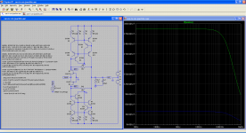
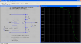
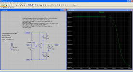
For Joachim's circuit in post #99, THD is 0.0016% in Spice.
- Without 4x 370R loading resistor, THD is improved to 0.0012% for lesser voltage swing at input FET drains.
- Without the 4 helper BJT, THD is increased to 0.003%.
- Without 2x 50k feedback resistor is THD is 0.0021%.
So plenty of choices, whether to go for simplicity or the last few dBs THD.
We'll stay with the Wilson mirror for now.
I think I had a thinking error with Calvin's circuit. I think I get it now about the biasing.
My apologies to Calvin.
Still, my prejudice remains against exponential devices.
But I guess the real test is a listening test.
See if I have time to put a proto board together, using 3 separate supplies.
Patrick
Joachim,
A member of my team did the sim, not me ....")
I think it is just simple Spice with perfect resistors, so noise is not taken into account.
If you want to know more, please send me a email via the forum.
I'll get you in touch with him directly so that you don't have to talk via me.
Of course I want to be on the copy list to know what is going on ...
Shall be travelling tomorrow, so no email then.
Patrick
A member of my team did the sim, not me ....
I think it is just simple Spice with perfect resistors, so noise is not taken into account.
If you want to know more, please send me a email via the forum.
I'll get you in touch with him directly so that you don't have to talk via me.
Of course I want to be on the copy list to know what is going on ...
Shall be travelling tomorrow, so no email then.
Patrick
Piersma, i would call that a compound input stage. I have played around with the principle.
I like the adjustable input offset. Of cause your stage needs a floating supply plus a conventional supply. My idea with the output buffer has the same unconvenience.
What are the 10nF caps for or do i read it wrong ? I would use a high value electrolytic
in that place to lower noise by 3dB.
Here is a paper that describes the compound input stage :
http://www.linearaudio.nl/Miscellaneous/smedegaard 4217 aes pp.PDF
The BJT models are just those from manufacturer.
The JFET models are based on those in the forum, but with the Vth adjusted to match Idss.
If you already have a basic model, you can compare the constants to those in post#104 & 109.
The text is clearly visible.
I don't have the asc files with me. Otherwise no problem to post them.
Patrick
The JFET models are based on those in the forum, but with the Vth adjusted to match Idss.
If you already have a basic model, you can compare the constants to those in post#104 & 109.
The text is clearly visible.
I don't have the asc files with me. Otherwise no problem to post them.
Patrick
perhaps this help:Guys, how do I calculate R and C values for a given DAC chip? I'm interested in trying out Sen.
Digi Scoop 1
You mean which DAC? PCM1794A (7.8 mA p-p) and PCM1798 (4 mA p-p). I'd like to know how to tune Sen parameters for these DACs.What do you intend to use ?
Firstly, a declaration of interest.
I published these articles and make these evaluation kits available to encourage you to understand circuits, apart from building them.
"You" meaning the DIY forum in general and not a particular person specifically.
So if you were looking for a simple answer to enable you to go and build without understanding, you might well be disappointed with my answers.
So be warned.
But take PCM1798 as an example.
They have not published any internal circuits, which makes life somewhat difficult.
But table 3, fig. 24 & 29 gives you sufficient information to make an educated guess.
I don't have these parts; I have not measured them. So don't take my answers as definitive.
I am just illustrating how to do it, rather than giving you a definitive solution.
Table 3 says at no signal, there is a negative current of -3.5mA.
That means that the sum of Idss of the upper FETs has to be larger than that of the lower FETS, in order to supply this 3.5mA.
In the SEN circuit, you might need to add a source resistor to the lower FETs and trim that for zero DC out.
It also says that Vout of U2 in Fig.24 is -2.87V with no signal and Riv=820R.
That implies the output voltage of the DAC is at 0V.
(Vout - 3.5mA x 820R = -2.87V, hence Vout = 0V)
So the gates of the JFETs are still to be connected to Gnd.
To work out R_iv.
Assume you would like 2Vrms per phase, as most standard CD players.
2Vrms is approx. 5.6 p-p. The output current is 4mA p-p.
So R_iv = 5.6 / 4 = 1.4k.
As I said in the article, the JFET bias should be at least 2x the p-p output current amplitude.
So 8mA total Idss is minimum.
Hope the explanation is clear enough that you can work out for yourself for PCM1794.
Patrick
Thank your for detailed explanation, Patrick. The algorithm is perfectly clear, I sure can recalculate for 1794. Still don't understand how the circuit works, though, but that's my personal problem.
Is my understanding correct that I should use unipolar 18V voltage source and not a bipolar +/- 18?
I also wonder what's the point of doubling JFETs in Sen vs Cen. Scrolled through the thread but didn't see an explanation. Could you explain in few words?
Is my understanding correct that I should use unipolar 18V voltage source and not a bipolar +/- 18?
I also wonder what's the point of doubling JFETs in Sen vs Cen. Scrolled through the thread but didn't see an explanation. Could you explain in few words?
Last edited:
- Home
- Source & Line
- Digital Line Level
- Zen -> Cen -> Sen, evolution of a minimalistic IV Converter