How much DC-offset is acceptable?
Even if Hugh say 200mV, I am sure he would not feel good about it.
I say less than 100mV or even 50mV is a wish.
I know Nelson Pass once got this question if 100mV was okay?
He told he wanted less.
I did a test.
I replaced IRF9610 for one ZVP4424 in SPICE.
Everything else in circuit was left equal for the compare.
THD went up from 0.019% to 0.021%
ZVP3310A got THD 0.020%
So we get
0.019% THD IRF9610
0.020% THD ZVP3310A
0.021% THD ZVP4424
This tells, at least me, that these 3 perform very much alike.
We should not expect almost any noticable difference
if we chose one or another MOSFET of these 3.
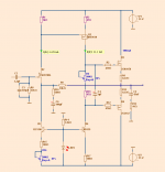
Here is the Official Fetzilla
that was used to test MOSFET:
Even if Hugh say 200mV, I am sure he would not feel good about it.
I say less than 100mV or even 50mV is a wish.
I know Nelson Pass once got this question if 100mV was okay?
He told he wanted less.
I did a test.
I replaced IRF9610 for one ZVP4424 in SPICE.
Everything else in circuit was left equal for the compare.
THD went up from 0.019% to 0.021%
ZVP3310A got THD 0.020%
So we get
0.019% THD IRF9610
0.020% THD ZVP3310A
0.021% THD ZVP4424
This tells, at least me, that these 3 perform very much alike.
We should not expect almost any noticable difference
if we chose one or another MOSFET of these 3.
Here is the Official Fetzilla
that was used to test MOSFET:
Attachments
Last edited:
20mV or less for me.
I'm curious - why 20mV or less ?
Any higher and the speakers get pushed out/pulled in enuf to cause significant rise in distortion, and a constant dc on the voice coil heats it up.
In some speakers, a dc offset can actually destroy the magnet, rendering the speaker useless.
Also dc offset affects the amplifiers distortion figures.
Last but not least, i've heard that amplifier designs putting out more than 50mV dc offset are either bad designs or poorly trimmed/built.
In some speakers, a dc offset can actually destroy the magnet, rendering the speaker useless.
Also dc offset affects the amplifiers distortion figures.
Last but not least, i've heard that amplifier designs putting out more than 50mV dc offset are either bad designs or poorly trimmed/built.
1) Heating up speakers:
50mV / 4 ohms = 0.0125amps
0.0125amps x 50mV = 0.000625 watts
0.625mW heats up the voice coil ? turning on the central heating would be more significant.
2) Polarised loudspeakers - mmmmm possibly an issue - what type of speaker are destroyed ?
3) I cannot see how up to 1 volt DC offset would significantly affect distortion figures.
Can you show us any evidence of this ?
4) Your last point doesn't mean anything unless one of the three above is clearly demonstrated.
My question remains - does anyone really know what harm some DC offset can do ?
It may be it not good but I have yet to hear an even vaguely convincing augument against it.
Agree with NP. If 100mV is the figure, I want less.... I'd prefer less than 50mV. That said, Mike's figures are 100% correct and reflect the trivial dissipations in speaker voice coils at anything up to 1V of offset. Any cone excursion one way or the other will simply hike up H2 and H3, nothing more, adding a bit of body to the sound. It is absolutely nothing to get your knickers in a knot about.
Offset drift in this circuit is largely thermal, caused by Vgs changes in the VAS as it warms. A CCS also drifts with temperature. Heatsinking helps here, particularly at 20mA, but essentially there is nothing wrong with setting it to -50mV at switch on, and watching it reach equilibrium after 25 minutes to 0mV +/-10mV. If you eschew the large fb shunt cap, then offset control would require a servo, which is not complex, but simply more circuitry to accommodate.
I will await further comments on the sound before signing off on the pcb, which now includes two individual power supply bridges with UFSR diodes and all associated filter caps on the pcb for easy assembly onto a 300mm x 75mm flat back heatsink. This can be used for your selection of Iq at anything up to 1A.
Hugh
Last edited:
A CCS also drifts with temperature
Yes... some are NTC , others PTC. In a proper design , this might be a valid consideration. It might be possible to pair the active VAS with it's antithesis
( CCS wise). Just a thought. Lots of variants possible here (2Q , CFP , 2D , LED - or FET !!) also the option of separate sources. Arctic to tropics <5mv - why not ? Most sources can be coaxed to be either coefficient with minimal additional components.
** as a sidenote - I know this won't really affect sonics , but if my meter sees too many mv's , I know something is astray'. Dang perfectionist

Lineup, docO, all.
First things, first. Please don't think I am not willing to try any devices you suggest DocO. I am not ignoring your suggestions. The reason I have used the 9610 and 3310s is because I already have them here from my aleph 3 days, lots of them in fact.
I am not averse to trying anything you suggest, it's just a matter of getting the parts. I live in a remotish area. I place very large orders once in a while and any parts that get suggested here may make it into the next order if it seems warranted.
As it turns out, I have some very special parts coming that I think will blow everything else out of the water, so stay tuned.
Lineup, I would be a bit dubious about those models for the fets. The new versions of the 9610 are not very linear at low currents - ever since Vishay or whoever it was took out IRF. This has been documented in the forums by Nelson pass. Again, I am using them because I have them. Plus, the rather agricultural nature and high capacitance of these devices seems to make them more stable in the circuit, which is convenient.
I have had the privilege of casting an eye over an initial layout of hugh's PCB and it is looking very good. His significant experience in the commercial amplifier market is adding a certain professionalism and robustness to the design an amateur may omit.
Last edited:
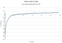
Direct Coupled DC Offset Test Results
Mikelm.
Here are the DC offset test results for the direct coupled circuit I posted. As you can see it did not stabilise within an hour, though it was better than I expected.
I must admit, this is the first thorough test I have done with the mosfet VAS, so I don't know if this drift is caused by the fet VAS or the direct coupling or a bit of both.
The last circuit I did a thorough test for had the BJT VAS which may have worked in opposition to the other devices in the circuit.
To answer your question I like mostly 70s rock and modern female acoustic vocals, however I'll listen to nearly anything.
In particular I never get tired of Pink Floyd.
Attachments
SWF,
This seems pretty high.... too much, in fact.
The drift indicates quite a big change in Vgs on the VAS, but there may also be changes for the input jfet as well. Both will compound the offset drift.
Is there a heatsink on the VAS? Reducing its temperature range will reduce the drift.
Cheers,
Hugh
This seems pretty high.... too much, in fact.
The drift indicates quite a big change in Vgs on the VAS, but there may also be changes for the input jfet as well. Both will compound the offset drift.
Is there a heatsink on the VAS? Reducing its temperature range will reduce the drift.
Cheers,
Hugh
It's funny, many here, including me to some extent, have the "feeling" that DC voltage offset should be low but I have yet to see / hear any concrete evidence why.
So, for the sake of clarity of understanding for us all, can anyone explain clearly & fully, giving solid facts or figures rather than vague feelings or preferences, why DC offset should be less than 100mV ?
Answers in two main groups please.
1) sound quality
2) safety of amp or speaker
I'm happy to learn something here if there is something to learn, but I would also be happy if we can blow an audio "urban myth" out the window.
mike
Last edited:
Swordfishy,
The change in Vgs of VAS MF may act to cancel DC offset at o/p so we don't necessarily have to try to reduce it.
As someone said already the key to DC offset is current in the i/p stage.
If we want to achieve low DC offset without a servo (which we know is possible because TimA has already done it)
The first thing we need to know is:
How the current in the i/p stage changes with time.
Then we need to establish what final adjustment is needed to that current to restore low DC at o/p
Then we need to go figure.
Let's examine offset drift in SWF's design.
As Mike identifies, it's controlled from the source voltage of the input device, which in turn works off the gate, which is fixed by a bias voltage. Set the gate voltage, and the source will follow, though there is always some mischief between gate and source on any device. Typically it will change by around 2mV for each Celsius rise in temperature.
Let us assume the output is a 0mV offset, that is, perfectly nulled.
The entire current from the input device, the jfet, is passed through the feedback resistor to the output. This current enters the jfet through the drain, and originates at the point where the gate/source resistor on the VAS, in this case 1K, is attached to the rail.
The value of this VAS gate/source resistor, 1K, fixes the current through it when the amp is operating. The VAS operates at around 4V of Vgs, so since the gate passes no current 4mA must flow from the positive rail, though this resistor, to the drain of the input jfet, and then out of the source and into the series feedback resistor to the output of the amplifier.
Now, consider what happens as the VAS warms. This is a mosfet, and the bias voltage changes far, far more than it does for a bipolar or jfet device. It's Vgs drops precipitously, let's say from 4V to 3.6V.
This reduces the input stage current from 4mA to 3.6mA since any fixed voltage across a resistor comprises a current generator. With an amended stage current, the jfet will also see a change in its Vgs, slightly lower in fact since the current is less, and this in turn will shift the potential at the jfet source up slightly, but this effect is secondary and lower since jfet biases are an order of magnitude lower than mosfet biases.
Of most significance is the reduced current through the series feedback resistor. Assuming it's 500R, what was once a voltage drop of exactly 2V leading to 0mV at the output, is now reduced to 1.8V, and in consequence, since the input stage bias voltage remains hopefully unchanged, we see a rise of 200mV in the output offset. In fact, any current change through the VAS gate/source resistor will also show up at the series feedback resistor, and since the ratio of these two resistors is 2:1, then the offset voltage change will always be exactly half the voltage change in Vgs at the VAS.
We have some options; one is to cool the VAS and keep it as close to room temp as possible; another is to use a different device whose bias voltage changes little with temperature (any bipolar is good here, such as a 2SC3423, which might change only about 60mV in a 30C rise).
A decision may be needed. My own preference would be to use a different VAS, and keep it well cooled.
BTW SWF, using another mosfet as CCS won't change things at all, since it is not the current through the CCS which is controlling proceedings; rather it is the current through the first stage, and this is controlled solely by the resistor between gate and source of the VAS.
Hope this explains things clearly,
Hugh
Last edited:
. . . there is always some mischief between gate and source on any device. Typically it will change by around 2mV for each Celsius rise in temperature.
This 2mV change is why I was thinking about achieving constant power across the i/p device - thus avoiding temperature changes with signal.
constant current + a hawksford cascode will achieve this but I accept that there may be other drawbacks . . . . but I still intent to explore this sometime soon.
But, Mike, that won't change things...... when you switch on the amp, it's cold, then, regardless of constant power or otherwise, it still warms up, moving the offset.
Nah, only one way around it. Either keep the VAS at room temperature - difficult - or use a servo. On my large NAKSA, the 100W//8R, I use a single transistor servo which keeps it within +/-5mV with a single one time adjustment.
Cheers,
Hugh
Nah, only one way around it. Either keep the VAS at room temperature - difficult - or use a servo. On my large NAKSA, the 100W//8R, I use a single transistor servo which keeps it within +/-5mV with a single one time adjustment.
Cheers,
Hugh
Hugh & all,
This is getting very confusing I think we should state if we are talking about DC linked or AC linked versions at the top of out posts.
Hugh,
In your explanation above you seem to be discussing an AC linked version because you say all of the i/p stage current flows to the o/p and with DC linking this surely is not the case.
Since Swordfishy is trying the DC version presently I am thinking to try and address the offset probelm without resorting to a servo.
( My Hawksford cascode idea has absolutely nothing to do with DC offset. )
cheers
mike
- Status
- This old topic is closed. If you want to reopen this topic, contact a moderator using the "Report Post" button.
- Home
- Amplifiers
- Solid State
- JFET input, MOSFET VAS, LATERAL output = Perfect!!